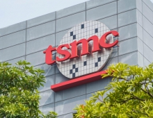
Infineon and TSMC Extend Technology And Production Partnership Agreement
Infineon Technologies AG and Taiwan Semiconductor Manufacturing Company today announced that they are extending their development and production partnership to a 65nanometer (nm) embedded flash (eFlash) process technology targeting next generation automotive, chip card and security applications.
Based on the agreement, Infineon and TSMC will jointly develop 65nm process technologies for eFlash microcontrollers (MCUs) that fulfill the quality requirements of the automotive industry, as well as the demanding security requirements of the chip card and security markets.
The partnership extension with TSMC is in line with Infineons strategy to outsource manufacturing and to engage in technology co-development for 65nm and smaller geometry processes. The 65nm eFlash technology for automotive applications supports the high degree of functional integration required that drive the performance and features called for in upcoming safety and emission standards. The 65nm eFlash technology for chip card and security applications will support Infineons focus on tailored security for applications in the smart card form factor and beyond.
Process and product qualification for security MCUs is scheduled for the second half of 2012. Automotive MCU qualification and production start is scheduled for the first half of 2013. Infineons 32-bit TriCore family MCUs will be the first automotive products produced on the 65nm eFlash process. Ultimately, TSMC will manufacture Infineons broad range of security microcontrollers that feature contact-based, contact-less or dual interface.
Infineon and TSMC have compiled more than a decade-long partnership covering several Infineons applications, such as industrial and wireline. The companies are aleady into a manufacturing agreement to use TSMC 65nm low-power technology for Infineons products employed in mobile devices.
Infineon is one of two market leaders that both hold a 9.5% share of the worldwide automotive electronics market in 2008, worth about US$18.3 billion. Infineon is the number one chip card semiconductor vendor, with 25.5 percent of the worldwide market valued at US$2.4 billion in 2008.
TSMC is the only dedicated foundry to offer 0.25-micron and 0.18-micron embedded flash IP that meet AEC-Q100 specification.