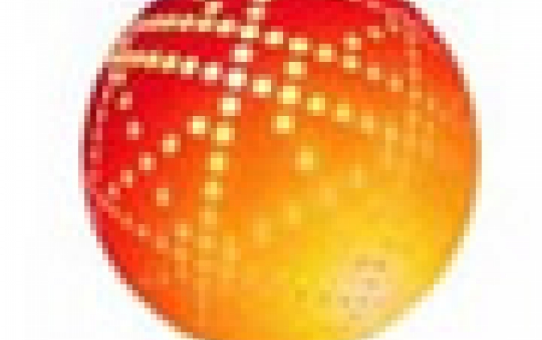
GLOBALFOUNDRIES Fab 8 To Enable 3D Chip Stacking at 20nm and Beyond
At its Fab 8 campus in Saratoga County, NY, GLOBALFOUNDRIES has begun installation of a special set of production tools to create Through-Silicon Vias (TSVs) in semiconductor wafers processed on the company's 20nm technology platform.
The TSV capabilities will allow stacking of multiple chips on top of each other, providing another avenue for delivering the demanding requirements of tomorrow's electronic devices.
Essentially vertical holes etched in silicon and filled with copper, TSVs enable communication between vertically stacked integrated circuits. For example, the technology could allow circuit designers to place stacks of memory chips on top of an application processor, which can significantly increase memory bandwidth and reduce power consumption.
At leading-edge nodes, the adoption of 3D stacking of integrated circuits is being viewed as an alternative to traditional technology node scaling at the transistor level. However, as new packaging technologies are introduced, the complexity of chip-package interaction is going up significantly and it is increasingly difficult for foundries and their partners to be able to deliver end-to-end solutions that meet the requirements of the broad range of leading-edge designs.
"To help address these challenges on new silicon nodes, we are engaging early with partners to jointly develop packaging solutions that will enable the next wave of innovation in the industry," said Gregg Bartlett, chief technology officer of GLOBALFOUNDRIES. "Our approach is broad and collaborative, giving customers maximum choice and flexibility, while delivering cost savings, faster time-to-volume, and a reduction in the technical risk associated with developing new technologies. With the installation of TSV capabilities for 20nm technology in Fab 8, we are adding an important capability that will be supplemented by our joint development and manufacturing partnerships with companies across the semiconductor ecosystem, from design to assembly and test."
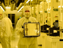
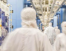
GLOBALFOUNDRIES' new Fab 8 campus stands as the largest semiconductor foundry in the United States. The site is focused on manufacturing at 32/28nm and below, with 20nm technology development well underway. The first full-flow silicon with TSVs is expected to start running at Fab 8 in Q3 2012.
Essentially vertical holes etched in silicon and filled with copper, TSVs enable communication between vertically stacked integrated circuits. For example, the technology could allow circuit designers to place stacks of memory chips on top of an application processor, which can significantly increase memory bandwidth and reduce power consumption.
At leading-edge nodes, the adoption of 3D stacking of integrated circuits is being viewed as an alternative to traditional technology node scaling at the transistor level. However, as new packaging technologies are introduced, the complexity of chip-package interaction is going up significantly and it is increasingly difficult for foundries and their partners to be able to deliver end-to-end solutions that meet the requirements of the broad range of leading-edge designs.
"To help address these challenges on new silicon nodes, we are engaging early with partners to jointly develop packaging solutions that will enable the next wave of innovation in the industry," said Gregg Bartlett, chief technology officer of GLOBALFOUNDRIES. "Our approach is broad and collaborative, giving customers maximum choice and flexibility, while delivering cost savings, faster time-to-volume, and a reduction in the technical risk associated with developing new technologies. With the installation of TSV capabilities for 20nm technology in Fab 8, we are adding an important capability that will be supplemented by our joint development and manufacturing partnerships with companies across the semiconductor ecosystem, from design to assembly and test."
GLOBALFOUNDRIES' new Fab 8 campus stands as the largest semiconductor foundry in the United States. The site is focused on manufacturing at 32/28nm and below, with 20nm technology development well underway. The first full-flow silicon with TSVs is expected to start running at Fab 8 in Q3 2012.