Cadence Announces Tapeout of 14 nm Test-Chip
Cadence announced today the tapeout of a 14-nanometer test-chip featuring an ARM Cortex-M0 processor implemented using IBM's FinFET process technology.
The 14-nanometer ecosystem and chip are significant milestones of a multi-year agreement between ARM, Cadence and IBM to develop systems-on-chip (SoCs) at the advanced process nodes of 14 nanometers and beyond. SoCs designed at 14 nanometers with FinFET technology offer the promise of a significant reduction in power consumption.
"This chip represents a major milestone for advanced node process technology, achieved through tight collaboration among experts at the three companies," said Chi-Ping Hsu, senior vice president, Silicon Realization Group at Cadence. "FinFET designs offer significant advantages to the design community, but also require advanced foundry support, IP and EDA technology to meet the considerable challenges. Cadence, IBM and ARM are collaborating to address these challenges and develop an ecosystem that can support 14-nanometer FinFET development for a broad range of production designs."
The chip was developed to validate the building blocks of foundation IP for 14-nanometer design. In addition to the ARM processor, SRAM memory blocks and other blocks were included that provide the characterization data necessary for foundation IP development for FinFET-based ARM Artisan physical IP.
ARM design engineers incorporated an ARM Cortex-M0 processor using 14-nanometer FinFET technology built on IBM's silicon-on-insulator (SOI) technology, which offers an optimal performance/power profile. A 14-nanometer double patterning and FinFET support methodology was employed, with engineers using Cadence technology to design the FinFET 3D transistor chip.
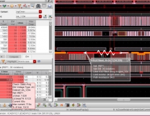
To succeed, engineers required support for 14-nanometer and FinFET rule decks, as well as enhanced timing analysis. The chip was implemented using the Cadence Encounter Digital Implementation (EDI) System with ARM 8-track 14-nanometer FinFET standard cell libraries designed with Cadence Virtuoso tools. EDI System provides digital capability required for implementing designs based on 14-nanometer FinFET-based DRC rules, and incorporates new GigaOpt optimization technology to realize power and performance benefits offered by FinFET technology. In addition, the solution also uses production-proven double patterning-correct implementation capabilities. Encounter Power System, Encounter Timing System and Cadence QRC Extraction provide 14 nm timing and power signoff capabilities supporting 14-nanometer FinFET structures.
"This chip represents a major milestone for advanced node process technology, achieved through tight collaboration among experts at the three companies," said Chi-Ping Hsu, senior vice president, Silicon Realization Group at Cadence. "FinFET designs offer significant advantages to the design community, but also require advanced foundry support, IP and EDA technology to meet the considerable challenges. Cadence, IBM and ARM are collaborating to address these challenges and develop an ecosystem that can support 14-nanometer FinFET development for a broad range of production designs."
The chip was developed to validate the building blocks of foundation IP for 14-nanometer design. In addition to the ARM processor, SRAM memory blocks and other blocks were included that provide the characterization data necessary for foundation IP development for FinFET-based ARM Artisan physical IP.
ARM design engineers incorporated an ARM Cortex-M0 processor using 14-nanometer FinFET technology built on IBM's silicon-on-insulator (SOI) technology, which offers an optimal performance/power profile. A 14-nanometer double patterning and FinFET support methodology was employed, with engineers using Cadence technology to design the FinFET 3D transistor chip.
To succeed, engineers required support for 14-nanometer and FinFET rule decks, as well as enhanced timing analysis. The chip was implemented using the Cadence Encounter Digital Implementation (EDI) System with ARM 8-track 14-nanometer FinFET standard cell libraries designed with Cadence Virtuoso tools. EDI System provides digital capability required for implementing designs based on 14-nanometer FinFET-based DRC rules, and incorporates new GigaOpt optimization technology to realize power and performance benefits offered by FinFET technology. In addition, the solution also uses production-proven double patterning-correct implementation capabilities. Encounter Power System, Encounter Timing System and Cadence QRC Extraction provide 14 nm timing and power signoff capabilities supporting 14-nanometer FinFET structures.