|
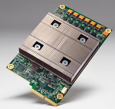
Google claims that a Tensor Processing Unit (TPU), a dedicated hardware for running machine- learning applications like voice recognition, is more powerful than Intel's Haswell CPUs and Nvidia Tesla K80 GPUs.
ATensor processing unit (or TPUs) is a custom application-specific integrated circuits (ASIC) developed specifically for machine learning.
Today, Google released a comparison of the TPU's performance and efficiencies compared with Haswell CPUs and Nvidia Tesla K80 GPUs, in a datacenter environment.
Google's paper evaluates a Tensor Processing Unit (TPU)? deployed in datacenters since 2015 that accelerates the inference phase of neural networks (NN). The heart of the TPU is a 65,536 8-bit MAC matrix multiply unit that offers a peak throughput of 92 TeraOps/second (TOPS) and a large (28 MiB) software-managed on-chip memory.
Google says that the TPU's deterministic execution model is a better match to the 99th-percentile response-time requirement of its NN applications than are the time-varying optimizations of CPUs and GPUs
(caches, out-of-order execution, multithreading, multiprocessing, prefetching, ...) that help average throughput more than guaranteed latency. The lack of such features helps explain why, despite having myriad MACs and a big memory, the TPU is relatively small and low power. Google compares the TPU to a server-class Intel Haswell CPU and an Nvidia K80 GPU, which are contemporaries deployed in the same datacenters.
Google's workload, written in the high-level TensorFlow framework, uses production NN applications (MLPs, CNNs, and LSTMs) that represent 95% of its datacenters' NN inference demand.
Google claims that despite low utilization for some applications, the TPU is on average about 15X -30X faster than its contemporary GPU or CPU, with TOPS/Watt about 30X - 80X higher. Moreover, using the GPU's
GDDR5 memory in the TPU would triple achieved TOPS and raise TOPS/Watt to nearly 70X the GPU and 200X the CPU.
The TPU chip size can fit in a hard drive slot within a data center rack according to Google Distinguished Hardware Engineer Norm Jouppi, who joined Google three years ago and has been one of the chief architects of the MIPS processor- possibly the best processor achitecture ever.

Despite its multitude of matrix multiplication units, the TPU does not have any stored program; it simply executes instructions sent from the host. The DRAM on the TPU is operated as one unit in parallel because of the need to fetch so many weights to feed to the matrix multiplication unit.
More details about the test
In Google's tests, a Haswell Xeon E5-2699 v3 processor with 18 cores running at 2.3 GHz using 64-bit floating point math units was able to handle 1.3 Tera Operations Per Second (TOPS) and delivered 51 GB/sec of memory bandwidth; the Haswell chip consumed 145 watts and its system (which had 256 GB of memory) consumed 455 watts when it was busy.
The TPU, by comparison, used 8-bit integer math and access to 256 GB of host memory plus 32 GB of its own memory was able to deliver 34 GB/sec of memory bandwidth on the card and process 92 TOPS - a factor of 71X more throughput on inferences, and in a 384 watt thermal envelope for the server that hosted the TPU.
Google also examined the throughput in inferences per second that the CPUs, GPUs, and TPUs could handle with different inference batch sizes and with a 7 milliseconds.
With a small batch size of 16 and a response time near 7 milliseconds for the 99th percentile of transactions, the Haswell CPU delivered 5,482 inferences per second (IPS), which was 42 percent of its maximum throughout (13,194 IPS at a batch size of 64) when response times were allowed to go as long as they wanted and expanded to 21.3 millisecond of the 99th percentile of transactions. The TPU, by contrast, could do batch sizes of 200 and still meet the 7 millisecond ceiling and delivered 225,000 IPS running the inference benchmark, which was 80 percent of its peak performance with a batch size of 250 and the 99th percentile response coming in at 10 milliseconds. |