Researchers have managed to create a tiny transistors that are not based on any semiconductor material. Instead, a piece of plastic with a substrate of metal powders on top can operate as a semiconductor switching between conducting and an insulating states.
Electronic devices have been getting smaller, and smaller, allowing chip makers to place millions of transistors on a single silicon chip. However, at the rate the current technology is progressing, in 10 or 20 years, transistors won't be able to get any smaller.
Scientists have experimented with different materials and designs for transistors to address these issues, always using semiconductors like silicon.
This time, researchers at the Michigan Technological University have come up with something different that might open the door to a new age of electronics.
"The idea was to make a transistor using a nanoscale insulator with nanoscale metals on top," said physicist Yoke Khin Yap of
Michigan Technological University. "In principle, you could get a piece of plastic and spread a handful of metal powders on top to make the devices, if you do it right. But we were trying to create it in nanoscale, so we chose a nanoscale insulator, boron nitride nanotubes, or BNNTs for the substrate."
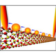
Yap?s team had figured out how to make virtual carpets of BNNTs,which happen to be insulators and thus highly resistant to electrical charge. Using lasers, the team then placed quantum dots (QDs) of gold as small as three nanometers across on the tops of the BNNTs, forming QDs-BNNTs. BNNTs are the perfect substrates for these quantum dots due to their small, controllable, and uniform diameters, as well as their insulating nature. BNNTs confine the size of the dots that can be deposited.
In collaboration with scientists at Oak Ridge National Laboratory (ORNL), they fired up electrodes on both ends of the QDs-BNNTs at room temperature, and something interesting happened. Electrons jumped very precisely from gold dot to gold dot, a phenomenon known as quantum tunneling.
"Imagine that the nanotubes are a river, with an electrode on each bank. Now imagine some very tiny stepping stones across the river," said Yap. "The electrons hopped between the gold stepping stones. The stones are so small, you can only get one electron on the stone at a time. Every electron is passing the same way, so the device is always stable."
Yap's team had made a transistor without a semiconductor. When sufficient voltage was applied, it switched to a conducting state. When the voltage was low or turned off, it reverted to its natural state as an insulator.
Furthermore, there was no "leakage": no electrons from the gold dots escaped into the insulating BNNTs, thus keeping the tunneling channel cool.
Yoke Khin Yap has filed for a full international patent on the technology.