
ARM has announced the availability for evaluation and licensing of its Artisan physical IP platform for the 7nm 7FF FinFET process from TSMC and a design win at that level with Xilinx Inc.
The IP set does not include support for extreme ultraviolet (EUV) lithography, which is expected to be deployed later.
The physical IP platform is available for tape outs in 1H17, and some engineering samples are expected in 2017, according to Ron Moore, vice president of marketing in the physical design group at ARM. However, it is not clear that there is a performance, power or area benefit in selecting the 7FF process over the 10FF process.
The 10FF was a marked scaling over 16FF+ that could produce a 20 percent speed increase at the same power, or more than 40 percent power reduction at the same speed. But it came at the cost of the increased use of double patterning.
TSMC has two nodes that are different - 16/14 and 10/7. For TSMC 7nm is the next generation from 10nm. But there are additional challenges such as lay-out rules and the electrical properties of transistors. You can expand that list to include process variation, routability, analysis for sign-off, timing variation and electromigration. And at 7nm without EUV there will be a requirement for triple patterning.
"We will have to redefine our cells to take account of EUV but 7FF is based on immersion lithography," said Moore.
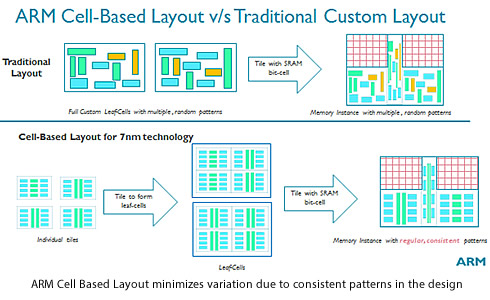
The ARM Artisan platform not only uses the Front End of Line (FEOL) device to provide performance, but also pays special consideration to the Back End of Line (BEOL). In 7nm technology, this could be the difference between a good SoC and an excellent SoC because unlike previous technology nodes, it's the BEOL that determines the quality of your performance and results, not just the FEOL device. The unique characteristics of the 7FF process technology meant that we had to invent a new memory development methodology, thus the introduction of memory compilers utilizing a cell based layout. This new memory architecture provides for more consistent patterns in the memory layout, thereby minimizing variation. Minimizing variation leads to less design margin and better memory PPA for use in the SoC.
As metallization becomes more challenging logic routability is critical, especially at 7nm FinFET, to determining the performance, power, and area (PPA) of a SoC. Solving routability is not limited to just tackling congestion, you also need to pay special attention to IR (voltage drop) and EM (electromigration). As the process design rules have gotten tighter going from 16/14nm FinFET to 7nm FinFET, the parasitic electrical properties have made it more challenging and complex to design a power grid. "A good power grid can help you get significantly better performance and save both power and area in SoC designs," accotding to Moore.

He says that te ARM Artisan Power Grid Architect (PGA) simplifies the development of the power grid; with the knowledge of Artisan logic libraries encapsulated in PGA, the power grid creation is correct-by-construction. As a result, Moore says that a knowledgeable SoC designer can create a power grid that meets their needs within a matter of hours, versus the several days and iterations it may have taken previously.
However, all of the extra work does mean that an area reduction is not guaranteed.
"The transistors may be smaller, but that does not necessarily mean smaller cells," said Moore. As has been seen in the past scaling of the front-end-of-line (FEOL) does not produce an area benefit if it is hobbled by an earlier generation of back-end-of-line (BEOL). There are in effect multiple levels of optimisation; transistor, standard cells, IP blocks, cores.
"Area savings can be realized at the core level but it is not a trivial task. It is about optimization for the combination of performance, power consumption and area [PPA]." For example ARM has also had to invent a memory compiler that could utilize a cell-based layout - rather than a more simplistic grid - to minimize variation. Minimizing variation leads to less design margin and better memory PPA.
Moore added that with the move to 7FF comes an increased susceptibility to ubiquitous background radiation and a requirement for additional circuitry. "At 7nm FinFET all memory compilers are ECC and use hardware detect and repair mechanisms. At 16nm it was only for critical or high performance memories with more reliance on software correction.
The big picture is that moving from 16nm FinFET to 7nm FinFET you can keep the power budget and improve performance. Similarly, if you move from 16nm to 7nm you can keep a performance level of about 3GHz and drop the power by 20 percent, Moore said.
The queston here is whether there are enough benefits at 7nm to make the extra engineering and what the impact on yield will be.