Intel Details Ivy Bridge, Explores Foundry Business
Intel gave more details of the 22nm Ivy Bridge chip, at the the International Solid-State Circuits Conference in San Francisco. The company also opened its chip manufacturing facilities to third-party customers, starting with Tabula Inc.
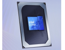
Starting with ISSCC 2012 event, Intel has spent effort to create the die of the Ivy Bridge chip modular, in order to easy create different flavors of it. The chip's largest die includes four x86 cores and a large graphics block. It can be chopped using automated generation tools to create versions with two cores or a smaller graphics block.
The company plans to release at least four major variants of the chip which packs 1.4 billion transistors into 160-mm-square in its largest version. The processors to use Intel's 22-nm tri-gate technology.
The first Ivy Bridge chip targets a range of desktop, notebook, embedded, and single-socket server systems with up to 8 Mbytes cache. It also integrates a memory controller and graphics, now upgraded to support DDR3L DRAMs and Microsoft DirectX 11.0 graphics APIs.
The processor also packs 20 channels of PCI Express Gen 3 interconnect and a Displayport controller. The Displayport block supports three simultaneous displays including one 1.6 GHz and two 2.7 GHz links with four lanes each.
Ivy Bridge is Intel's first client chip to support low power 1.35V DDR3L and DDR power gating in standby mode. It handles up to 1,600 MTransfers/s as well as 1.5V DDR3.
Seperately, at the Ethernet Technology Summit, Santa Clara, Calif., Tabula Inc. confirmed previous speculation that it is implementing a family of 3PLD products manufactured by Intel using its 22nm manufacturing process featuring 3-D Tri-Gate transistors and co-optimized packaging technology. This is made possible by a manufacturing access agreement between Tabula Inc., and Intel Custom Foundry, a division of the Technology and Manufacturing Group of Intel. The 3PLD family will be based on Tabula?s 3D Spacetime architecture and will deliver solutions for network infrastructure systems requiring high-bandwidth data flows such as Switches, Routers, Packet Inspection appliances, and other high-performance systems. The combination of process and architecture will allow Tabula to produce programmable circuits that consume significantly less chip area than circuits implemented with traditional FPGA fabrics.
Intel is exploring whether it can branch out as a foundry by opening its chip manufacturing facilities to more third-party customers. The company in the past had exclusively retained manufacturing facilities for its own chips, but late last year said it would make FPGAs (field-programmable gate arrays) for Achronix Semiconductor.
Although Intel doesn't expect to be a large-scale foundry company like its rivals, there could be strategic advantages in opening up its manufacturing facilities.
Intel's 22-nm manufacturing facilities are considered more advanced than its top contract manufacturing rivals including TSMC (Taiwan Semiconductor Manufacturing Co.), UMC (United Microelectronics Corp.) and GlobalFoundries.
Intel is the only company offering chips with power-efficient 3D transistors, which could be attractive to third parties because it is more power-efficient than planar transistor designs. TSMC is expected to implement 3D transistors eventually.


