Micron Unveils 16-Nanometer Flash Memory Technology
Micron Technology today announced that it is sampling 16-nanometer (nm) process technology, enabling the industry's smallest 128-gigabit (Gb) multi-level cell (MLC) NAND Flash memory devices.
 The 16nm node is not only the leading Flash process, but it is also the most advanced processing node for any sampling semiconductor device.
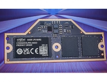
Micron's 128Gb MLC NAND Flash memory devices are targeted at applications like consumer SSDs, removable storage (USB drives and Flash cards), tablets, ultrathin devices, mobile handsets and data center cloud storage. The new 128Gb NAND Flash memory provides the greatest number of bits per square millimeter and lowest cost of any MLC device in existence. In fact, the new technology could create nearly 6TB of storage on a single wafer.
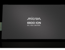
Micron has started sampling the 16nm, 128Gb MLC NAND with select partners and plans to be in full production in 4Q13. The company is also developing a new line of solid-state drive (SSD) solutions based on these devices and expects to ship SSDs with 16nm Flash in 2014.


