Semiconductor Industry Moves To 300mm Wafer Fabs
Nearly all new fab upgrade and construction activity has to do with 300mm wafer processing, but there is still plenty of life remaining in 200mm fabs according to data IC Insights.
It is obvious that moving to 300mm wafers provide significant cost savings. However, not all semiconductor devices are able to take advantage of the cost savings. Therefore, fabs running 200mm wafers will continue to be profitable for many more years to produce several types of ICs such as specialty memories, image sensors, display drivers, microcontrollers, and analog products (200mm fabs are also used for manufacturing MEMS-based "non-IC" products such as accelerometers). These devices can be manufactured in fully depreciated 200mm fabs that were previously used to make ICs that are now produced on 300mm wafers.
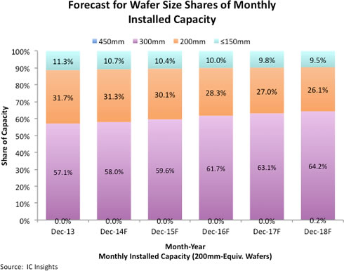
According to data released by IC Insights, between December 2013 and December 2018, the share of the industry's monthly wafer capacity represented by 200mm wafers is expected to drop from 31.7% to 26.1%. However, in terms of the actual number of wafers used, an increase in 200mm wafers is forecast through 2015 followed by a slow decline through the end of 2018.

Wafers measuring ≤150mm are also forecast to increase slowly throughout the forecast period to meet the growing demand for products such as general-purpose analog chips that can be cost-effectively manufactured on the smaller wafers.
For the most part, 300mm fabs will continue to be limited to production of high-volume, commodity-type devices like DRAMs and flash memories, complex logic and microcomponent ICs with large die sizes, image sensors and power management devices; and products manufactured by foundries, which can fill a 300mm fab by combining wafer orders from many sources. IC Insights projects that more than 105 wafer fabs will be producing 300mm wafer fabs in 2018. This number includes pilot- and volume-production class fabs, but not R&D facilities. Also, "phases" are counted as separate fabs (e.g., TSMC?s Fab 14 currently has four phases for a total of 180K wafers/month).
According to data released by IC Insights, between December 2013 and December 2018, the share of the industry's monthly wafer capacity represented by 200mm wafers is expected to drop from 31.7% to 26.1%. However, in terms of the actual number of wafers used, an increase in 200mm wafers is forecast through 2015 followed by a slow decline through the end of 2018.

Wafers measuring ≤150mm are also forecast to increase slowly throughout the forecast period to meet the growing demand for products such as general-purpose analog chips that can be cost-effectively manufactured on the smaller wafers.
For the most part, 300mm fabs will continue to be limited to production of high-volume, commodity-type devices like DRAMs and flash memories, complex logic and microcomponent ICs with large die sizes, image sensors and power management devices; and products manufactured by foundries, which can fill a 300mm fab by combining wafer orders from many sources. IC Insights projects that more than 105 wafer fabs will be producing 300mm wafer fabs in 2018. This number includes pilot- and volume-production class fabs, but not R&D facilities. Also, "phases" are counted as separate fabs (e.g., TSMC?s Fab 14 currently has four phases for a total of 180K wafers/month).


