ARM-based Intel Stratix 10 FPGA Launches for 5G, NFV and Data Centers
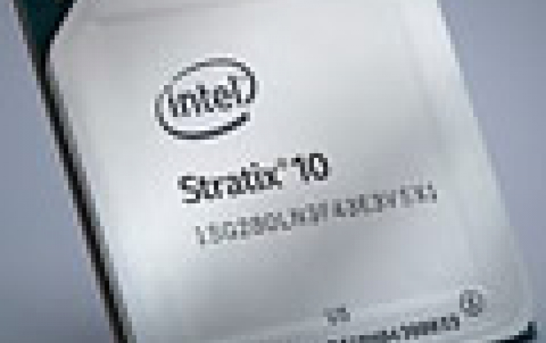
Intel has begun shipping its Intel Stratix 10 SX FPGA, a high-end FPGA family with an integrated quad-core ARM Cortex-A53 processor.
Stratix 10 SoCs are Intel's (formerly Altera) third-generation SoC FPGA family. Stratix 10 SoCs, manufactured on Intel's 14 nm process technology, combine a quad-core ARM Cortex-A53 MPCore hard processor system operating up to 1.5 GHz with the HyperFlex core fabric architecture to create what Intel calls "the highest performance and power efficient SoC FPGA in the industry."
The Stratix 10 SoCs HPS architecture includes a System Memory Management Unit, which enables hardware virtualization across the processor and FPGA domains. Stratix 10 SoCs add a Cache Coherency Unit to provide one-way (I/O) cache coherency with the Cortex-A53 MPCore. Stratix 10 SoCs also include up to 10 TFLOPS of hardened floating-point digital signal processing (DSP) blocks, embedded high-speed transceivers, hard memory controllers, and protocol intellectual property (IP) controllers - all in a single package.
By integrating the FPGA and the ARM processor, Intel says that the Stratix 10 SX FPGAs provide "an ideal solution" for 5G wireless communication, software defined radios, secure computing for military applications, network function virtualization (NFV) and data center acceleration.
For NFV applications that consolidate and deliver the networking components needed to support a fully virtualized infrastructure, Intel Stratix 10 SX FPGAs can handle the high-speed data path while integrated processors enable the low latency transactions needed to manage flow tables for control plane processing. With hardware acceleration, Intel Stratix 10 SX FPGAs provide a heterogeneous computing environment to create optimized, low latency accelerators. In secure computing applications, integrated processors make it much more difficult to snoop software operations thereby helping keep data secure. These devices also enable general purpose utility processing to extend convenience and form factor reduction in high-end systems.
Intel's customers can implement their designs today with the Intel Stratix 10 SX FPGA, using the Intel SoC FPGA Embedded Development Suite (Intel SoC FPGA EDS), a tool suite for embedded software development. It comprises development tools, utility programs, and design examples to jump-start firmware and application software development.
The Intel SoC FPGA EDS also enables Intel's customers to utilize the ARM Development Studio 5 (DS-5) Intel SoC FPGA Edition to code, build, debug and optimize their applications.
Intel SoC Feature Comparison
| Feature | Arria V SoC | Arria 10 SoC | Stratix 10 SoC |
|---|---|---|---|
| Process Technology | 28 nm TSMC | 20 nm TSMC | 14 nm Intel Tri-Gate |
| Processor | Dual-core ARM Cortex-A9 MPCore | Dual-core ARM Cortex-A9 MPCore | Quad-core ARM Cortex-A53 MP Core |
| Maximum Processor Performance | 1.05 GHz | 1.5 GHz | 1.5 GHz |
| Logic Core Performance | 300 MHz | ~500 MHz | 1 GHz |
| Power Dissipation | 1X | 0.6X | 0.3X |
| Logic Density Range | 350 - 462K logic element (LE) | 160 - 660K LE | 500K LE - 5.5M LE |
| Embedded Memory | 23 Mb | 39 Mb | 229 Mb |
| 18 x 19 Multipliers | 2,136 | 3,356 | 11,520 |
| Maximum Transceivers | 30 | 48 | 144 |
| Maximum Transceiver Data Rate (Chip to Chip) | 10 Gbps | 17.4 Gbps | 30 Gbps |
| Memory Devices Supported | DDR3 SDRAM @ 533 MHz | DDR4 SDRAM @ 1,200 MHz DDR3 SDRAM @ 1066 MHz LPDDR3 @ 800 MHz QDR IV SRAM @ 1066 MHz QDR II+ SRAM @ 633 MHz Hybrid Memory Cube |
DDR4 SDRAM @ 1,333 MHz DDR3 SDRAM @ 1066 MHz QDR IV SRAM @ 1066 MHz QDR II+ SRAM @ 633 MHz Hybrid Memory Cube |
| Hard Protocol IP | 2 EMACs PCI Express (PCIe) Gen2 x8 |
3 EMACs |
3 EMACs PCI Express Gen3 X 8 10/40G BaseKR- forward error correction (FEC) Interlaken physical coding sublayer (PCS) |
| Security | Advanced Encryption Standard (AES) | AES encryption Authentication based on Elliptic Curve Digital Signature Algorithm (ECDSA), Public key infrastructure with layered hierarchy for root of trust, Anti-tamper enhancements |
AES-256/SHA-256 bitsream encryption/authentication, physically unclonable function (PUF), ECDSA 256/384 boot code authentication, multi-factor key infrastructure with layered hierarchy for root of trust, side channel attack protection |


