Intel Showcases 10 nm Updates, a new aspect for Moore's Law, FPGA Progress and 64-Layer 3D NAND for Data Center
Intel delivered updates at its Technology and Manufacturing Day held in Beijing, China, on Sept. 19, with disclosures to include power and performance updates for Intel's 10 nm process, high-level plans for Intel's first 10 nm FPGA, and the shipment of 64-layer 3D NAND for data center applications.
"Intel manufacturing processes advance according to Moore's Law, delivering ever more functionality and performance, improved energy efficiency and lower cost-per-transistor with each generation," said Stacy Smith, group president of Manufacturing, Operations and Sales. "We are pleased to share in China for the first time important milestones in our process technology roadmap that demonstrate the continued benefits of driving down the Moore's Law curve."
Smith added that Intel's ability to advance Moore's Law - to make products less expensive and more capable every year - is the company's core competitive advantage. Smith said that Intel's role has been, and will continue to be, that of the technology leader driving Moore's Law, and that Intel "has about a three-year lead in process technology."
"Sixteen nanometer, 14, 10, 7 - it looks like a horse race. The problem is that those figures, which are numbers that used to have real, physical meaning, no longer mean anything at all. There needs to be a metric that captures a process' ability to deliver usable transistors to chip designers," Smith added.
Smith admitted that there are some specific challenges that must be solved soon with 7 nm, but still Intel today has line of sight to 7 and 5 nm. "We may not know exactly which approaches will prove best for 5 nm yet, but our culture thrives on those challenges. It has for generations," he said.
He added that Intel will continue to take new nodes into production. In fact, the company announced a new foundry offering: an ultra-low-power 22 nm FinFET process.
New "metric" for Moore's Law
Intel Senior Fellow Mark Bohr described how the company realizes the Moore's law today, using a metric that captures a process' ability to deliver usable transistors to chip designers.
Bohr presented specification updates showing Intel's 10 nm is a full generation ahead of other "10 nm" technologies in terms of both transistor density and transistor performance.
Historically, the industry has been following Moore's law, and has named each successive process node approximately 0.7 times smaller than the previous one -a linear scaling that implies a doubling of density. Thus, there was 90 nm, 65 nm, 45 nm, 32 nm - each enabling the packing of twice the number of transistors in a given area than was possible with the previous node.
But recently - perhaps because of the increasing difficulty of further scaling - some companies have abandoned this rule, yet continued to advance node names, even in cases where there was minimal or no density increase. "The result is that node names have become a poor indicator of where a process stands on the Moore's Law curve," Bohr said.
One simple metric is gate pitch (gate width plus spacing between transistor gates) multiplied by minimum metal pitch (interconnect line width plus spacing between lines), but this doesn't incorporate logic cell design, which affects the true transistor density. Another metric, gate pitch multiplied by logic cell height, is a step in the right direction with regard to this deficiency. "But neither of these takes into account some second order design rules. And both are not a true measure of actual achieved density because they make no attempt to account for the different types of logic cells in a designer's library. Furthermore, these metrics quantify density relative to the previous generation," Bohr said,
Intel's executive said that there is a need for an absolute measure of transistors in a given area (per mm2). At the other extreme, simply taking the total transistor count of a chip and dividing by its area is not meaningful because of the large number of design decisions that can affect it - factors such as cache sizes and performance targets can cause great variations in this value.
Bohr resurrected a metric that was used in the past. It is based on the transistor density of standard logic cells and includes weighting factors that account for typical designs. While there is a large variety of standard cells in any library, Intel takes one ubiquitous, very simple one - a 2-input NAND cell (4 transistors) - and one that is more complex but also very common: a scan flip flop (SFF). This leads to a previously accepted formula for transistor density:

(The weightings 0.6 and 0.4 reflect the ratio of very small and very large cells in typical designs.)
Bohr says that every chip maker, when referring to a process node, should disclose its logic transistor density in units of MTr/mm2 (millions of transistors per square millimeter) as measured by this simple formula. Reverse engineering firms can readily verify the data.
There is one important measure missing: SRAM cell size. Given the wide variety of SRAM-to-logic ratios in different chips, it is best to report SRAM cell size separately, next to the NAND+SFF density metric.
"By adopting these metrics, the industry can clear up the node naming confusion and focus on driving Moore's Law forward," Bohr concluded,
Intel claims that its 10 nm technology "has the world's tightest transistor and metal pitches, created with hyper scaling, for the highest density in the industry." Hyper scaling is a term used by Intel to describe the 2.7x logic transistor density improvement attained on the company's 14 nm and 10 nm processes. And, for the first time, Intel's "Cannon Lake" 10 nm wafer was on public display.
The minimum gate pitch of Intel's 10 nm process shrinks from 70 nm to 54 nm and the minimum metal pitch shrinks from 52 nm to 36 nm. These smaller dimensions enable a logic transistor density of 100.8 mega transistors per mm2, which is 2.7x higher than Intel's previous 14 nm technology and is approximately 2x higher than other industry 10 nm technologies.

Intel says that its 10 nm process delivers up to 25 percent better performance and 45 percent lower power than the previous 14 nm technology. Intel also claims that its 10nm also has a performance lead over other industry "10nm" technologies. An enhanced version of the 10 nm process, called 10++, can boost the performance an additional 15 percent or reduce power by 30 percent.
Intel Custom Foundry offers the Intel 10 nm process through two design platforms: 10GP (general purpose) and 10HPM (high performance
mobile). These platforms include broad silicon-validated IP portfolios, ARM Libraries and POP Kits, and fully integrated turnkey foundry services and support.
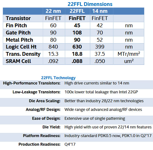
Bohr also provided power and performance updates for Intel's 22FFL, a lower-power FinFET technology for mobile applications first introduced at Intel's Technology and Manufacturing Day in March in San Francisco. The updates included best-in-class CPU performance of more than 2 Ghz with ultra-low power of more than 100x lower leakage compared with the previous 22GP (general purpose) technology. The 22FFL process also delivers drive currents on par with Intel's 14 nm transistors while delivering better area scaling than industry 28 nm/22 nm planar technologies.

In addition, a 22FFL wafer was on public display for the first time.
Intel unveiled high-level plans for its coming generation of FPGAs using the 10 nm process technology and foundry platform. Introduced under the code name "Falcon Mesa," the FPGA will offer "new levels of performance "to support the growing bandwidth demands of data center, enterprise and networking environments.
Falcon Mesa 10nm FPGAs will continue Intel's FPGA transceiver technology:
- 112 Gbps serial transceiver links to support the most demanding bandwidth requirements in next-generation data center, enterprise and networking environments.
- Latest peripheral device interconnect including PCI Express Gen4 x16 support with data rates up to 16 GT/s per lane for next-generation data centers.
The new FPGA family will also build upon several technologies from the current Intel Stratix 10 14 nm FPGA family:
- Intel's next-generation Embedded Multi-Die Interconnect Bridge (EMIB) packaging technology for system-in -package (SiP) integration. The second generation will be optimized for higher levels of transceiver performance alongside a monolithic FPGA fabric
- Next-generation high bandwidth memory (HBM) support, a DRAM memory architecture that delivers 10x the performance of discrete memory solutions in a smaller form factor with lower power consumption.
- Next generation of Intel HyperFlex architecture, which uses registers, called hyper-registers, throughout the FPGA, optimized for leading performance on 10 nm. The second generation of Intel HyperFlex architecture, combined with Intel Quartus Prime and
high-level design tools, promise to deliver the highest in performance and productivity required for next-generation systems
Intel did not disclose any additional details or any timeline for product availability of the new 10nm FPGAs.
During the Intel Developer Forum in San Francisco in August 2016, Intel Custom Foundry announced an agreement with ARM to accelerate the development and implementation of ARM SoCs on Intel's 10 nm process. The results of this collaboration were highlighted with the display of a 10 nm test chip wafer containing ARM Cortex-A75 CPU cores implemented with industry standard design flows enabling performance in excess of 3 GHz.
Intel also announced that it is shipping of the first 64-layer, triple level cell (TLC), 3D NAND SSD (solid state drive) for data center applications. The product has been shipping to "select top-tier" cloud service providers since early August. Intel says the product will be made more broadly available by the end of this year.
$1 Billion investment in the AI Ecosystem
Intel also talked about Artificial Intelligence and how it would bring significant new opportunities to transform business - from retail to healthcare to manufacturing.
To drive AI innovation, Intel is making investments spanning technology, R&D and partnerships with business, government, academia and community groups. The company has invested in startups like Mighty AI, Data Robot and Lumiata through our Intel Capital portfolio.
Intel has a larg selection of options for its customers to choose from. The Intel Nervana AI portfolio includes:
- Intel Xeon Scalable family - providing highly scalable processors for evolving AI workloads and our purpose-built silicon for intensive deep learning training, code-named "Lake Crest"
- Intel Mobileye - vision technologies for specialized use cases such as active safety and autonomous driving
- Intel FPGAs - programmable accelerators for deep learning inference
- Intel Movidius - low-power vision technology provides machine learning at the edge


