Self-assembly Technique Could Solve Miniaturization Chip Making Issues
Researchers from the Massachusetts Institute of Technology and the University of Chicago have come up with a technique for self-assembling that could be used to create tiny wiring lines onto small chip geometries.
For the last few decades, microchip manufacturers have been on a quest to find ways to make the patterns of wires and components in their microchips ever smaller, in order to fit more of them onto a single chip and thus continue the relentless progress toward faster and more powerful computers. That progress has become more difficult recently, as manufacturing processes bump up against fundamental limits involving, for example, the wavelengths of the light used to create the patterns.
A team of researchers at MIT and in Chicago has found an approach that could break through some of those limits and make it possible to produce some of the narrowest wires yet, using a process with the potential to be economically viable for mass manufacturing with standard types of equipment.
The new findings are reported this week in the journal Nature Nanotechnology, in a paper by postdoc Do Han Kim, graduate student Priya Moni, and Professor Karen Gleason, all at MIT, and by postdoc Hyo Seon Suh, Professor Paul Nealey, and three others at the University of Chicago and Argonne National Laboratory. While there are other methods that can achieve such fine lines, the team says, none of them are cost-effective for large-scale manufacturing.
The new approach includes a technique in which polymer thin films are formed on a surface, first by heating precursurs so they vaporize, and then by allowing them to condense and polymerize on a cooler surface.
Today's methods for producing features smaller than about 22 nanometers (billionths of a meter) across generally require either extreme ultraviolet light with very expensive optics or building up an image line by line, by scanning a beam of electrons or ions across the chip surface - a very slow process and therefore expensive to implement at large scale.
According to Gleason, who is MIT's associate provost as well as the Alexander and I. Michael Kasser (1960) Professor of Chemical Engineering, the new process uses an integration of three existing methods. First, a pattern of lines is produced on the chip surface using well-established lithographic techniques, in which an electron beam is used to "write" the pattern on the chip.
Then, a layer of material known as a block copolymer - a mix of two different polymer materials that naturally segregate themselves into alternating layers or other predictable patterns - is formed by spin coating a solution. The block copolymers are made up of chain-like molecules, each consisting of two different polymer materials connected end-to-end.
"One half is friendly with oil, the other half is friendly with water," Kim explains. "But because they are completely bonded, they're kind of stuck with each other." The dimensions of the two blocks predetermine the sizes of periodic layers or other patterns they will assemble themselves into when they are deposited.
Finally, a top, protective polymer layer is deposited on top of the others using initiated chemical vapor deposition (iCVD). This top coat, it turns out, is a key to the process: It constrains the way the block copolymers self-assemble, forcing them to form into vertical layers rather than horizontal ones, like a layer cake on its side.
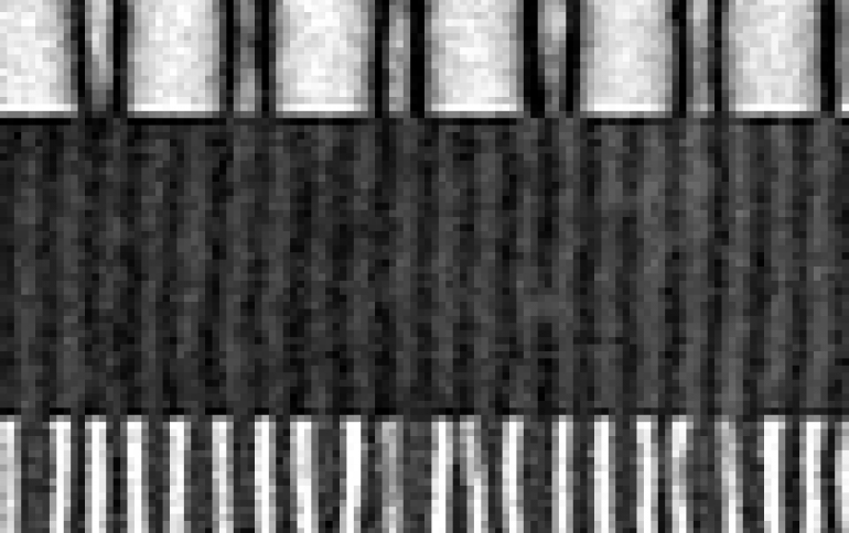
The underlying lithographic pattern guides the positioning of these layers, but the natural tendencies of the copolymers cause their width to be much smaller than that of the base lines. The result is that there are now four (or more, depending on the chemistry) lines, each of them a fourth as wide, in place of each original one. The combination of the lithographed layer and topcoat "controls both the orientation and the alignment" of the resulting finer lines, explains Moni.
Because the top polymer layer can additionally be patterned, the system can be used to build up any kind of complex patterning, as needed for the interconnections of a microchip.
Most microchip manufacturing facilities use the existing lithographic method, and the CVD process itself is a well-understood additional step that could be added relatively easily. Thus, implementing the new method could be much more straightforward than other proposed methods of making finer lines.
Being able to create sub-10-nanometer features with polymers could prove to be a major progress in the area of nanofabrication.