Stanford Researchers Develop A 'High-rise' Chip
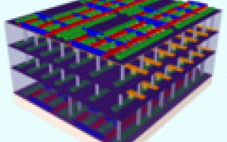
Stanford researchers are building layers of logic and memory into "skyscraper" chips that are smaller, faster, cheaper and taller, promising to leapfrog the performance of the single-story logic and memory chips on today's circuit cards. At a IEDM conference in San Francisco, a Stanford team revealed how to build high-rise chips and showcased a four-layer prototype. The bottom and top layers were logic transistors. Sandwiched between them were two layers of memory. The vertical tubes were nanoscale electronic "elevators" that connect logic and memory, allowing them to work together to solve problems.
Stanford researchers said that their approach ends these the "jam" issues among the wires connecting logic and memory. Many thousands of nanoscale electronic "elevators" would move data between the layers much faster, using less electricity, than the bottleneck-prone wires connecting single-story logic and memory chips today.
The researchers' innovation leverages three breakthroughs.
The first is a new technology for creating transistors. The researchers used carbon nanotubes – or CNT – transistors, which do not suffer from the common "electricity leaks" (heat) met in silicon transistors. Imagine that nearly 2 billion CNTs could fit within a human hair. The researchers managed to make some of the highest performance CNT transistors ever built, by packing enough CNTs into a small enough area to make a useful chip.
They started by growing CNTs the standard way, on round quartz wafers. Then they added their trick. They created what amounts to a metal film that acts like a tape. Using this adhesive process they lifted an entire crop of CNTs off the quartz growth medium and placed it onto a silicon wafer.
This silicon wafer became the foundation of their high-rise chip.
But first they had to fabricate a CNT layer with sufficient density to make a high-performance logic device. So they went though this process 13 times, growing a crop of CNTs on the quartz wafer, and then using their transfer technique to lift and deposit these CNTs onto the silicon wafer.
Moreover, the Stanford team showed that they could perform this technique on more than one layer of logic as they created their high-rise chip.
The second innovation the researchers used was a new type of computer memory that lends itself to multi-story fabrication.
The Stanford team fabricated memory using titanium nitride, hafnium oxide and platinum. This formed a metal/oxide/metal sandwich. Applying electricity to this three-metal sandwich one way causes it to resist the flow of electricity. Reversing the electric jolt causes the structure to conduct electricity again.
The change from resistive to conductive states is how this new memory technology creates digital zeroes and ones. The change in conductive states also explains its name: resistive random access memory, or RRAM.
Wong designed RRAM to use less energy than current memory, leading to prolonged battery life in mobile devices.
Inventing this new memory technology was also the key to creating the high-rise chip because RRAM can be made at much lower temperatures than silicon memory.
The third is a technique to build these new logic and memory technologies into high-rise structures in a radically different way than previous efforts to stack chips.
Subhasish Mitra, a Stanford associate professor of electrical engineering and of computer science, said that the research was at an early stage, but the design and fabrication techniques were scalable, adding that further development of the architecture could lead to computing performance that is much, much greater than anything available today.


