Breaking News

Intel at Computex 2026 Industry-Leading 245TB Micron 6600 ION Data Center SSD Now Shipping be quiet! introduces Dark Rock Pro 6 and Dark Rock 6 XPG Unveils the World’s First Infinity Mirror Gaming Memory NOVAKEY RGB DDR5 ASUSTOR at Computex 2026

logo

  • Share Us
    • Facebook
    • Twitter
  • Home
  • Home
  • News
  • Reviews
  • Essays
  • Forum
  • Legacy
  • About
    • Submit News

    • Contact Us
    • Privacy

    • Promotion
    • Advertise

    • RSS Feed
    • Site Map

Search form

Alternatively to Moore's Law, New 2D Semiconductor Packs 3 Functions Into One Device

Alternatively to Moore's Law, New 2D Semiconductor Packs 3 Functions Into One Device

Enterprise & IT Jun 14,2017 0

Researchers have created a multifunctional device made of 2D tungsten diselenide (WSe2). This single semiconductor device can improve device functionality and reduce fabrication complexity, providing an alternative to scaling down the device's dimensions.

In the semiconductor industry, researchers typically try to improve the speed and efficiency of devices by scaling down the device's dimensions in order to fit more transistors, in accordance with Moore's law. However, this ongoing race cannot exponentially increase forever.

In a new study published in Nanotechnology, a team of researchers at SUNY-Polytechnic Institute in Albany, New York, has suggested that combining multiple functions in a single semiconductor device can improve device functionality and reduce fabrication complexity.

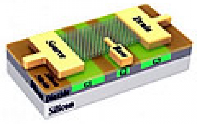
To demonstrate, the researchers designed and fabricated a reconfigurable device that can morph into three fundamental semiconductor devices: a p-n diode, a MOSFET, and a bipolar junction transistor.

In their paper, the researchers detail how they were able to develop new doping strategies with the recently discovered tungsten diselenide (WSe2) transition metal.

While such devices would typically be fabricated individually on modern chips, each requiring complex integration step, here the multiple functions device relies on multiple buried gates to achieve n- and p-channels, in effect dynamically selecting which carriers flow at the surface of the semiconductor.

This novel reconfigurable doping technique means a single device can be architected so as to operate differently depending on how the gates are controlled.

In the future, the researchers plan to further investigate the applications of these multifunctional devices.

Tags:
Previous Post
Nokia Unveils the World's Fastest Routers
Next Post
Samsung's new Smart Signage Display Portfolio Runs on TIZEN 3.0

Related Posts

Latest News

Intel at Computex 2026
Enterprise & IT

Intel at Computex 2026

Industry-Leading 245TB Micron 6600 ION Data Center SSD Now Shipping
Enterprise & IT

Industry-Leading 245TB Micron 6600 ION Data Center SSD Now Shipping

be quiet! introduces Dark Rock Pro 6 and Dark Rock 6
Cooling Systems

be quiet! introduces Dark Rock Pro 6 and Dark Rock 6

XPG Unveils the World’s First Infinity Mirror Gaming Memory NOVAKEY RGB DDR5
Gaming

XPG Unveils the World’s First Infinity Mirror Gaming Memory NOVAKEY RGB DDR5

ASUSTOR at Computex 2026
Enterprise & IT

ASUSTOR at Computex 2026

Popular Reviews

Akaso 360 Action camera

Akaso 360 Action camera

Dragon Touch Digital Calendar

Dragon Touch Digital Calendar

be quiet! Pure Loop 3 280mm

be quiet! Pure Loop 3 280mm

Noctua NF-A12x25 G2 fans

Noctua NF-A12x25 G2 fans

Soft2bet and the unseen hardware that makes instant play possible

Soft2bet and the unseen hardware that makes instant play possible

Crucial T710 2TB NVME SSD

Crucial T710 2TB NVME SSD

JSAUX 65Wh Rog Ally Battery

JSAUX 65Wh Rog Ally Battery

Introducing PriceHub

Introducing PriceHub

Main menu

  • Home
  • News
  • Reviews
  • Essays
  • Forum
  • Legacy
  • About
    • Submit News

    • Contact Us
    • Privacy

    • Promotion
    • Advertise

    • RSS Feed
    • Site Map
  • About
  • Privacy
  • Contact Us
  • Promotional Opportunities @ CdrInfo.com
  • Advertise on out site
  • Submit your News to our site
  • RSS Feed