Asus N6600GT AGP
3. A closer look
The Asus N6600GT is fabricated on a blue PCB following the reference design from NVidia. The GPU and its HSF have been rotated so that an extra chip can fit on the board.
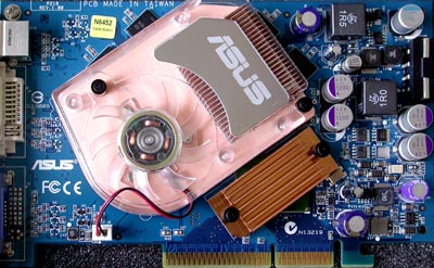 |
| The front side of the card.(click for hi-res). |
That chip is the HSI (short for High Speed Interconnect) and its purpose is to provide AGP support for the PCI-Express-native GPU used on the N6600GT.
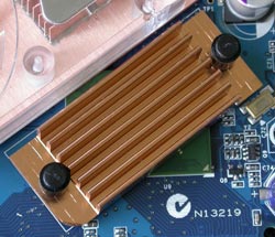 |
| The HSI chipset and its heatsink |
 |
| The front side of the card.(click for hi-res). |
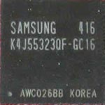
As you can see, all the memory parts are located on the front side of the 6600GT, leaving the back view empty. Even though the GPU fansink covers most of them, it doesn't actually come into contact with them since they don't need cooling.
 |
| Enlarged picture of the NV44 |
Removing the heatsink reveals the NV43 core on the N6600GT which is shown in the picture below.
 |
| Enlarged picture of the NV44 |
As with all AGP 6600GTs, the N6600GT also needs extra power for its circuits to operate correctly. A power socket exists near the right edge of the card where you have to plug in a molex power connector from your power supply.
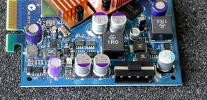 |
| The power socket for the N6600GT |
The Asus N6600GT can output 3 kinds of signals. One for TV-out, one DVI for TFT monitors and one for the standard CRT output.
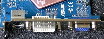 |
| S-Video, DVI and the standard VGA output |


