Cadence and Micron Prototype First DDR5 Memory
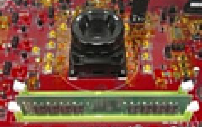
The DDR5 standard has not been finalized by JEDEC, but Cadence and micron have prototyped its first IP interface in silicon for a preliminary version of the DDR5 standard being developed in JEDEC.
The Cadence test chip was fabricated in TSMC's 7nm process and achieves a 4400 megatransfers per second (MT/sec) data rate, which is 37.5 percent faster than the fastest commercial DDR4 memory at 3200MT/sec.
The DDR5 standard is expected to be finalized by JEDEC sometime this summer. Getting designs into silicon can't wait until the standard is final before getting started. In principle, anything could change in the standard at any time until it is released, but everyone knows that the basic parameters are not going to change at this late date.
Cadence's test chip is containing next-generation memory interface IP based on the discussions of what is likely to be in DDR5, and Micron has produced prototype DRAM chips.
The test chip contains both the controller and PHY.
According to Cadence's Marc Greenberg, DDR5 is mostly a capacity solution, more than performance. As die get bigger, they get slower, due to all sorts of laws of physics. As you start building a 16Gb die in 1X memory technology, the distances start to get really long, which changes a lot of core timing parameters for the worse. Then the memory can't keep up with the CPU and so has to be overdesigned, making it bigger still, and so on. But everyone wants more memory in each server, for bigger datasets, bigger databases, bigger netlists, and so on. Cloud companies charge people for the memory in their instances and so there is a direct line from memory capacity to revenue. The DDR5 standard is aimed at making 16Gb die easier and to make vertical stacking easier. The speed of the core is unchanged, but the I/O is higher speed.
Once again with the caveat that the standard is not final, here is what it looks like DDR5 will specify:
- supply voltage will drop from 1.2V for DDR4 to 1.1V for DDR5
- data rates will run up to 6.4 Gbps eventually, 4.4Gbps initially
- on-die termination (pulled-up VDDQ) will be available for address buses, not just data buses
DDR4 today is not up to its maximum speed. Mainstream parts today are 2400 megatransfers per second. The high end is 2667. That will become mainstream this year, so we are still a couple of years from DDR4 reaching its maximum of 3200 megatransfers per second. DDR5 is expected to be 4400 megatransfers per second at first, which is what the Cadence test chip achieved. 6400 is the maximum but it will be many years before anyone gets there.


