Western Digital Introduces First 512 Gigabit 64-Layer 3D NAND Chip
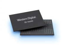
Western Digital has kicked off pilot production of the industry's densest 3D NAND flash chips, which stack 64 layers atop another and enable three bits of data to be stored in each cell.
The company's 512 Gigabit (Gb) three-bits-per-cell (X3) 64-layer 3D NAND (BICS3) is produced in Yokkaichi, Japan, with mass production expected in the second half of 2017.
Stacking NAND flash cells -- versus planar or 2D memory -enables manufacturers to increase density, which enables lower cost per gigabyte of capacity.
The latest 3D NAND chips have been used to create gum stick-sized SSDs with more than 3.3TB of storage and standard 2.5-inch SSDs with more than 10TB of capacity.
Samsung became the first company to announce it was mass-producing 3D flash chips in 2014. Their V-NAND technology originally stacked 32-layers of NAND flash. Samsung's V-NAND also crammed 3-bits per cell in what the industry refers to as triple-level cell (TLC) NAND or multi-level cell (MLC) NAND. Because Samsung uses TLC memory, its chips were able to store as much as Toshiba's original 48-layer 3D NAND chips, which stored 128Gbits or 16GB.
Intel and Micron also produce 3D NAND.
Western Digital's chip was developed jointly with the company's technology and manufacturing partner Toshiba. Western Digital first introduced initial capacities of the first 64-layer 3D NAND technology in July 2016 and the first 48-layer 3D NAND technology in 2015; product shipments with both technologies continue to retail and OEM customers.
Western Digital will present a technical paper on the advancement in high aspect ratio semiconductor processing that made this technology achievement possible on February 7, at the International Solid State Circuits Conference (ISSCC).

