Intel Shows Collaborative Mini-Bots, Brain-Inspired Computers and 5G at ISSCC 2019
Intel is presenting at ISSCC 2019 a series of innovations – from 5G networks to intelligent edge systems and robotic systems.
The International Solid-State Circuits Conference (ISSCC), is a forum on advanced circuit research and is held in San Francisco from Feb. 17-21.
Research presented includes:
Distributed Autonomous and Collaborative Multi-Robot System Featuring a Low-Power Robot SoC in 22nm CMOS for Integrated Battery-Powered Minibots
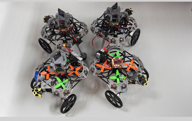
In this paper, Intel demonstrates a distributed, autonomous and collaborative multi-robot system featuring integrated, battery-powered, crawling and jumping minibots. For example, in a search and rescue application, four minibots collaboratively navigate and map an unknown area without a central server or human intervention, detecting obstacles and finding paths around them, avoiding collisions, communicating among themselves, and delivering messages to a base station when a human is detected.

Each minibot platform integrates: (i) a camera, LIDAR and audio sensors for real-time perception and navigation; (ii) a low-power custom robot SoC for sensor data fusion, localization and mapping, multi-robot collaborative intelligent decision-making, object detection and recognition, collision avoidance, path planning, and motion control; (iii) low-power ultra-wideband (UWB) radio for anchorless dynamic ranging and inter-robot information exchange; (iv) long-range radio (LoRa) for robot-to-base-station critical message delivery; (v) battery and PMIC for platform power delivery and management; (vi) 64MB pseudo-SRAM (PSRAM) and 1GB flash memory; and (vii) actuators for crawling and jumping motions.
Multi-robot systems, working collectively to accomplish complex missions beyond the capability of a single robot, have the potential to disrupt a wide range of applications ranging from search and rescue missions to precision agriculture and farming. The multi-bot systems can speed the time to perform a single task. For example, shortening time and latency for first responders during an emergency. However, advanced robotics and artificial intelligence have, to date, required large investment and intensive computational power. The development of these distributed, autonomous and collaborative minibots, which are operated by a system-on-chip that delivers efficiencies orders of magnitude beyond what was previously possible, represents the first step toward enabling the development of energy- and cost-efficient multi-robot systems.
5G Wireless Communication: An Inflection Point
5G presents an inflection point where wireless communication technology is driven by application and expected use cases, and where the network will set the stage for data-rich services and sophisticated cloud apps, delivered faster and with lower latency. Intel's paper highlights the architectures and technology innovations required to make 5G and beyond a reality.
Applying Principles of Neural Computation for Efficient Learning in Silicon
Intel’s Loihi processor implements a microcode-programmable learning architecture supporting a wide range of neuroplasticity mechanisms under study at the forefront of computational neuroscience. By applying many of the fundamental principles of neural computation found in nature, Loihi promises to provide highly efficient and scalable learning performance for supervised, unsupervised, reinforcement-based and one-shot paradigms. This talk describes these principles as applied to the Loihi architecture and shares Intel's preliminary results toward the vision of low-power, real-time on-chip learning.
Deep learning algorithms mainly used today in machine learning (ML) applications are very costly in terms of energy consumption, due to their large amount of required computations and large model sizes. Many issues, such as connectivity to the cloud, latency, privacy and public safety, could be resolved by establishing intelligent computing at the edge. By applying principles of neural computation to architecture, circuit and integrated design solutions, we could minimize the energy consumption and computational demand of edge learning systems.
Novel Memory/Storage Solutions for Memory-Centric Computing
Data and compute need to be brought closer together to avoid networking and storage protocol inefficiencies. This drives the demand for larger memory capacity, which is currently hindered by memory subsystem cost. In addition, the need for memory persistency will not only streamline storage protocols but will also significantly reduce bring-up time after system failure. Intel will discuss novel solutions for memory-centric architecture, with a focus on their value, performance and power efficiency.
- 3.6Mb 10.1Mb/mm2 Embedded Non-Volatile ReRAM Macro in 22nm FinFET Technology with Adaptive Forming/Set/Reset Schemes Yielding Down to 0.5V with Sensing Time of 5ns at 0.7V
- A 7Mb STT-MRAM in 22FFL FinFET Technology with 4ns Read Sensing Time at 0.9V Using Write-Verify-Write Scheme and Offset-Cancellation Sensing Technique
Intel gave further details on its technique for embedding spin-transfer torque (STT)-MRAM into devices using its 22nm FinFET process, pronouncing the technology ready for high-volume manufacturing.
The company said it has used a "write-verify-write" scheme and a two-stage current sensing technique to create 7Mb perpendicular STT-MRAM arrays in its 22FFL FinFET process.
The embedded MRAM technology achieves 10-year retention at 200°Celsius and endurance of more than 106 switching cycles, said Ligiong Wei, an Intel engineer who presented the paper Tuesday. The arrays have demonstrated write endurance of more than 1E06 cycles and read disturb error rate of more than 1E12 cycles, Wei said.
In addition to high endurance, the 22nm embedded MRAM technology boasts robust yields, with a bit yield rate of greater than 99.9%, according to Wei. However, manufacturing the devices requires error-correction code bits, increasing the size and power budget of the design, Wei said.
MRAM — which is a non-volatile memory technology — is considered a promising long term candidate to replace memory chip stalwarts DRAM and NAND flash, which face major scaling challenges as the industry moves to smaller nodes. But MRAM is also appealing as an embedded technology replacement for flash and embedded SRAM because of its fast read/write times, high endurance, and strong retention.
Wei said the eMRAM design is also tolerant of wide variations in supply voltage. The design achieves a 4ns read sensing time at 0.9V, but is also capable of 8ns read sensing time at 0.8V, she said.
In a separate ISSCC paper presented Tuesday, Intel also described the development of resistive RAM (ReRAM) as a low-cost option for embedded non-volatile memory for SoCs used in IoT and automotive. The embedded ReRAM technology — also implemented in a 22nm FinFET process — demonstrate what the company says is the smallest and highest density ReRAM subarray and material innovations to allow low-voltage switching without impact to transistor reliability.
With the explosive growth of memory-intensive workloads like machine learning, video capture/playback and language translation, there is interest in preforming some compute near memory, by placing logic inside the DRAM/NVM main-memory die (aka near-memory compute), or even doing the compute within the memory array, embedded within the compute die (aka in-memory compute). In either case, the motivation is to reduce the significant data movement between main/embedded memory and compute units, as well as to reduce latency by preforming many operations in parallel, inside the array.

