KIOXIA Launches The Software-Enabled Flash Technology
KIOXIA America, Inc. (formerly Toshiba Memory America, Inc.) today announced the introduction of Software-Enabled Flash (SEF), a new technology that combines software flexibility, host control and flash native semantics into a flash native API and purpose-built controller.
Targeted to data center directors, architects and developers, SEF technology makes flash easier to manage, more timely to deploy and more predictable in nature – putting the power in programmers’ hands.
KIOXIA's SEF is a new way for hyperscale users to directly control and manage flash devices through a software-driven Application Programming Interface (API). This API enables hyperscale service developers to control the behavior of software-enabled flash storage from their host applications.
With hyperscale computing redefining storage and virtualization, the race is on to orchestrate digital storage for cloud applications in a way that drives greater efficiency at scale. Effectively and efficiently utilizing flash for stable, predictable latency in ever-changing cloud workloads through direct host management of flash will quickly be critical to realizing these efficiencies.
KIOXIA designed SEF to free developers from narrowly defined “drive” behaviors by changing the relationship between solid-state storage and the host in cloud environments. SEF bypasses legacy HDD storage paradigms to unlock host control and enable the use of flash at its natural speed.
Additionally, SEF enables architects to freely and flexibly define storage behaviors between the host and the flash. The API abstracts generational differences, eliminating the need for developers to modify code with each new version of flash.
“As the inventor of flash memory, KIOXIA is perfectly positioned to introduce this game-changing approach to deploying flash at scale,” noted Eric Ries, SVP, Memory Storage Strategy Division (MSSD), KIOXIA America, Inc. “Our customers have been pushing for the ability to drive operational efficiency in the data center programmatically, and SEF technology will meet this need by placing access and control of flash directly in the hands of hyperscale programmers.”
SEF hardware is compliant with PCIe standards, enabling a large ecosystem and accelerating open innovation across multiple products.
SEF Features and Benefits
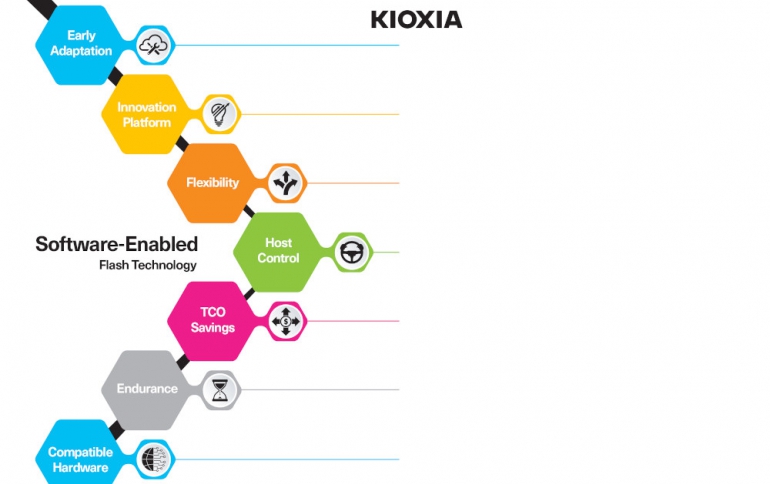
- Latency control over impacting algorithms, such as garbage collection and wear-leveling
- Host control over data placement and isolation
- Host control of workload isolation via system definable virtual devices and QoS domain(s)
- Physical address control over read processing (eliminates latency)
- Abstraction of flash memory generational and vendor differences to simplify adopting each new generation of flash memory

Features related to SEF hardware units can include the following:
- The flexibility in hardware to enable the use, reduction or elimination of device-side DRAM. For those deployments where host memory is preferred over device DRAM, the SEF API offers a Unified Write Buffer (UWB) capability that enables users to:
- Reduce or completely eliminate DRAM usage in favor of host memory usage
- Keep the conventional architecture that requires DRAM to be located at the drive side
- A ‘nameless write’ function that provides a flexible update of the L2P table and system-level optimization, enabling write data to be placed in the most optimized method for flash memory cell health and longevity
The SEF technology utilizes a software API that abstracts flash-based functions and enables host control over such SSD behaviors as latency management, data placement, tenant isolation and garbage collection.
The API is open-sourced and designed to enable software developers with the flexibility of adapting, developing, customizing or tuning flash memory to any application or storage need through software programming, and easily accessible to cloud applications, storage and developer communities.
The SEF hardware unit is architected to combine the most recent flash memory generation with a small onboard SoC controller that resides on a PCB module. As an option, the SEF architecture supports an on-device DRAM controller allowing the module to be populated with DRAM, based upon the needs of each hyperscale user. This combination of components comprise a SEF unit that is designed to deliver flash-based storage across a PCIe connection.
Behind the interface, individual SEF units handle all aspects of block and page programming (such as timing, ECC and endurance) for any type or generation of flash memory being used. SEF units also handle low-level read tasks that include error correction, flash memory cell health and life extension algorithms.


