ARM Announces 16-core Mali-T700 Series Of Graphics Processors
ARM has disclosed a new graphics chip design with many more processor cores than in the current generation. A future Mali-T760 graphics processing unit (GPU) -- due in products in the coming years -- will have up to 16 processor cores, ARM said Tuesday.
ARM announced the Mali-T720 GPU and the Mali-T760 GPUs.
Designed for premium mobile devices, the the ARM Mali-T720 GPU is designed for System on Chip (SoC) providers servicing high-growth markets. Licensees for the new ARM Mali GPUs include MediaTek, Rockchip and LG Electronics whose lead license was announced May this year.
"ARM Mali GPUs unit shipments have increased by more than 10x over the past two years and it is the unquestioned leader in Android devices today," said Pete Hutton, executive vice president and general manager, Media Processing Division, ARM. "The Mali-T700 Series family builds on our industry leadership in balancing power, area and functionality while incorporating new energy-saving features at the high-end and matching the time-to-market dynamics of the low-end. This combination gives our SoC partners a competitive edge, without compromising on performance and energy-efficiency."
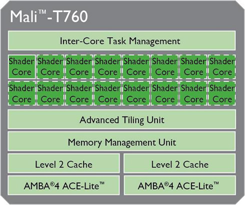
ARM claims that compared to the ARM Mali-T604 GPU, the new Mali-T760 offers an increase in energy efficiency and performance of approximately 400 percent. The SoC can scale up to 16 shader cores, which doubles the previous generation. A reduction in both the internal and SoC bandwidth utilization reduces energy consumption, enabled by ARM Frame Buffer Compression (AFBC) and Smart Composition. The result is a more than 50 percent reduction in total memory bandwidth utilization, compared to the Mali-T604 GPU. Its implementation has also been simplified through reduced wire count and layout congestion. ARM is also offering the ARM POP IP for ARM Mali-T760 GPU, which is expected to speed development and shorten implementation initially targeting TSMC 28HPM and TSMC 16FF process technologies.
ARM quotes a 1390Mtri/s, 11.2Gpix/s throughput for the Mali-T760 MP16 SoC, running at 695MHz and manufactured using the 28nm HPM process.
Mali GPUs are found in more than 50 percent of Android tablets and more than 20 percent of Android smartphones. The ARM Mali-T720 GPU is specifically tuned for the Android operating system and is derived from the Mali GPU found in the Samsung Galaxy Note 3. The Mali-T720 GPU is a cost-optimized solution targeted at entry-level Android devices.
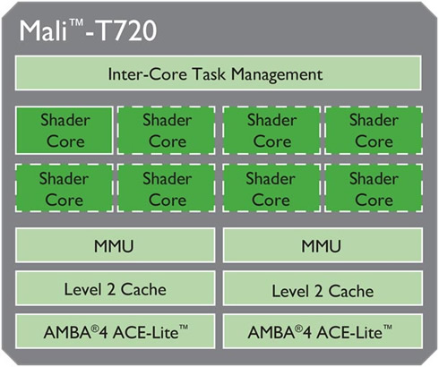
Compared to the ARM Mali-400 GPU, the new Mali-T720 promises to offer a greater than 150 percent energy efficiency increase. It can be implemented fast through high routing density and a simplified design. Its die area has been reduced by almost 30 percent while its graphics performance has been increased above 50% over previous cost optimized graphics processors, according to ARM. It also supports APIs OpenGL ES 3.0, OpenCL and RenderScript APIs and the POP IP for ARM Mali-T720 GPU offers area-optimized implementations balancing low power and performance initially targeting TSMC 28HPM process technology.
ARM quotes a 695Mtri/s, 5.6Gpix/s throughput for the Mali-T720 MP8 SoC, running at 695MHz and manufactured using the 28nm HPM process.
Designed for premium mobile devices, the the ARM Mali-T720 GPU is designed for System on Chip (SoC) providers servicing high-growth markets. Licensees for the new ARM Mali GPUs include MediaTek, Rockchip and LG Electronics whose lead license was announced May this year.
"ARM Mali GPUs unit shipments have increased by more than 10x over the past two years and it is the unquestioned leader in Android devices today," said Pete Hutton, executive vice president and general manager, Media Processing Division, ARM. "The Mali-T700 Series family builds on our industry leadership in balancing power, area and functionality while incorporating new energy-saving features at the high-end and matching the time-to-market dynamics of the low-end. This combination gives our SoC partners a competitive edge, without compromising on performance and energy-efficiency."

ARM claims that compared to the ARM Mali-T604 GPU, the new Mali-T760 offers an increase in energy efficiency and performance of approximately 400 percent. The SoC can scale up to 16 shader cores, which doubles the previous generation. A reduction in both the internal and SoC bandwidth utilization reduces energy consumption, enabled by ARM Frame Buffer Compression (AFBC) and Smart Composition. The result is a more than 50 percent reduction in total memory bandwidth utilization, compared to the Mali-T604 GPU. Its implementation has also been simplified through reduced wire count and layout congestion. ARM is also offering the ARM POP IP for ARM Mali-T760 GPU, which is expected to speed development and shorten implementation initially targeting TSMC 28HPM and TSMC 16FF process technologies.
ARM quotes a 1390Mtri/s, 11.2Gpix/s throughput for the Mali-T760 MP16 SoC, running at 695MHz and manufactured using the 28nm HPM process.
Mali GPUs are found in more than 50 percent of Android tablets and more than 20 percent of Android smartphones. The ARM Mali-T720 GPU is specifically tuned for the Android operating system and is derived from the Mali GPU found in the Samsung Galaxy Note 3. The Mali-T720 GPU is a cost-optimized solution targeted at entry-level Android devices.

Compared to the ARM Mali-400 GPU, the new Mali-T720 promises to offer a greater than 150 percent energy efficiency increase. It can be implemented fast through high routing density and a simplified design. Its die area has been reduced by almost 30 percent while its graphics performance has been increased above 50% over previous cost optimized graphics processors, according to ARM. It also supports APIs OpenGL ES 3.0, OpenCL and RenderScript APIs and the POP IP for ARM Mali-T720 GPU offers area-optimized implementations balancing low power and performance initially targeting TSMC 28HPM process technology.
ARM quotes a 695Mtri/s, 5.6Gpix/s throughput for the Mali-T720 MP8 SoC, running at 695MHz and manufactured using the 28nm HPM process.
| Mali-T760 | Mali-T720 | |
|---|---|---|
| Feature | Value / Description | |
| Anti-Aliasing | 4xFSAA, 8xFSAA, 16x MSAA / Hardware implemented Full Scene and Multiple Sample Anti-Aliasing | 4xFSAA, 8xFSAA / 4x Full Scene Anti-Aliasing (FSAA) with minimal performance drop |
| API Support | OpenGL ES 1.1, 2.0, 3.0 OpenCL 1.1 DirectX 11 RenderScript |
|
| Bus Interface | AMBA 4 ACE-LITE / Compatible with a wide range of bus interconnect and peripheral IP | |
| L2 Cache | Configurable 256kB-2048kB / 256kB-512kB for every 4 shader cores | Configurable
64kB-256kB / 32kB for MP1 configuration 64kB-128 kB for MP2 configurations 128kB-256kB for MP3 or bigger configurations |
| Memory System | Virtual Memory / Built-in Memory Management Unit (MMU) to support virtual memory | |
| Multi-Core Scaling | 1 to 16 cores / Optimized for high energy efficiency to address the high-end mobile and consumer device requirements | 1 to 8 cores / Optimized for high area and energy efficiency to address the mass mobile market requirements |
| Adaptive Scalable Texture Compression (ASTC) |
Low dynamic range (LDR) and high dynamic range (HDR). Supports both 2D and 3D images / ASTC offers a number of advantages over existing texture compression schemes by improving image quality, reducing memory bandwidth and thus energy use. | |
| ARM Frame Buffer Compression (AFBC) | 4x4 pixel block size / AFBC is a lossless image compression format that provides random access to pixel data to a 4x4 pixel block granularity. It is employed to reduce memory bandwidth both internally within the GPU and externally throughout the SoC | - |
| Transaction Elimination | 16x16 pixel block size / Transaction Elimination spots the identical pixel blocks between two consecutive render targets and performs a partial update to the frame buffer with the changed pixel blocks only, which reduces memory bandwidth and thus energy | |
| Smart Composition | 16x16 pixel block size / Smart Composition extends the concept of Transaction Elimination to every stage of UI composition. Identical pixel blocks of input surfaces are not read, not processed for composition and not written to final frame buffer | |

