Imec and ASML Demonstrate 24nm Pitch Lines With Single Exposure EUV Lithography
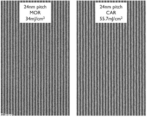
This week, at the SPIE Advanced Lithography Conference, imec and ASML announced a breakthrough in printing narrow 24 nanometer (nm) pitch lines, corresponding to the dimensions of critical back-end-of-line metal layers of a 3 nm technology node process.
By combining advanced imaging schemes, resist materials and optimized settings on ASML’s NXE:3400B system in imec’s cleanroom, the system is capable of printing lines/spaces at 24 nm pitch in a single exposure step.
This imaging performance enables imec’s ecosystem of resist and patterning partners to utilize the NXE:3400B as a platform for early material development for future process nodes that will be enabled by ASML’s next-gen EUV system, which will first ship in 2022. The EXE:5000 will have a numerical aperture of 0.55, much higher than the 0.33 of current EUV systems like NXE:3400B.
Steven Scheer, VP Advanced Patterning Process and Materials at imec:
“The innovation of imec and ASML in printing 24 nm pitch line spaces will provide the imec patterning ecosystem with the opportunity to test resist materials and provide process capabilities. The development of sensitive and stable resist materials will support the introduction of ASML’s next-gen EXE:5000 system.”
The NXE:3400B allows illumination of the mask under high incident angles. Under standard illumination the EUV mask tends to distort the wafer image under these high incident angles – creating poor resist profiles. Through a fundamental understanding of EUV mask effects, obtained from a joint imec/ASML study, the teams have found an innovative way to compensate for unwanted image distortion. In combination with an illumination optimization, this enabled the teams to print a pitch as small as 24 nm in a single EUV exposure step with a minimum exposure dose of 34J/cm2.
ASML’s NXE:3400B was installed in imec’s 300mm cleanroom in Q2 2019.
In addition, first 300 mm wafer high-NA lithography is anticipated this October using another key enabler, imec’s attosecond analytical and interference lithography lab. The AttoLab is critical to explore the molecular dynamics, at an attosecond scale, during exposure of photoresist to EUV ionizing radiation and, using interference lithography, it offers the first 300mm high-NA resist imaging capability to print features down to pitches of 8 nm. The AttoLab will improve the fundamental understanding of 0.55 NA resist imaging, and, complementary to the NXE:3400B, further supports the supplier ecosystem to accelerate the development of high-NA compatible materials before the introduction of ASML’s High NA EXE:5000.

