Infineon To Make FIrst Chips Out Of 300mm Wafers
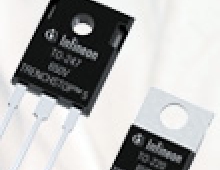
Infineon has got the go-ahead from customers to produce the world's first power chips on large, 300 mm (12 inch) thin wafers, the German company announced today.
In February, the company received the first customer go-aheads for products of the CoolMOS family produced by the 300-millimeter line at the Villach (Austria) site. Infineon says that the production process based on the new technology has completed qualification from start to finish and its customers have given the go-ahead.
"Infineon put its faith in this manufacturing technology very early on and continued to invest even in economically difficult times. We think and act with foresight and are now reaping the benefits: The qualification of our entire 300-millimeter line represents a veritable leap ahead of the competition," says Dr. Reinhard Ploss, CEO of Infineon Technologies AG. "300-millimeter thin-wafer manufacturing for power semiconductors will enable us, with the corresponding demand, to seize the opportunities that the market offers."
Thanks to their larger diameter compared to standard 200-millimeter wafers, two-and-a-half times as many chips can be made from each 300-mm wafer.
Power semiconductors from Infineon feature low energy loss and compact design. Although not much thicker than a sheet of paper, the chips have electrically active structures on the front and back. Thin-wafer technology is the basis for this.
The next step is for the present manufacturing concept for CoolMOS products, qualified from start to finish, with the front-end site Villach and assembly of the thin chips at the back-end site Malacca (Malaysia), to be expanded to the front-end site Dresden. Here the focus is on high-volume production in a fully automated 300-millimeter line. The basis for the processes required and the manufacturing technology is currently being developed in the company's research projects in Dresden. The technology transfer to Dresden is running on schedule and qualification of the first CoolMOS products will be completed in March. Shortly, in Villach more power semiconductor technologies will be transferred to the 300-millimeter line and produced. The development of the next power technology generation will focus on 300 instead of 200-millimeter technology.
"Our ability to innovate is the basis of our success - good ideas are turned into reality. In both Austria and in Saxony we have the necessary conditions for this: technological know-how, well-educated and highly motivated specialists and exemplary support from government policy," says Dr. Reinhard Ploss.


