JEDEC Publishes HBM3 Update to High Bandwidth Memory (HBM) Standard
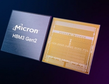
JEDEC Solid State Technology Association, the global leader in the development of standards for the microelectronics industry, today announced the publication of the next version of its High Bandwidth Memory (HBM) DRAM standard: JESD238 HBM3, available for download from the JEDEC website. HBM3 is an innovative approach to raising the data processing rate used in applications where higher bandwidth, lower power consumption and capacity per area are essential to a solution’s market success, including graphics processing and high-performance computing and servers.
Key attributes of the new HBM3 include:
Extending the proven architecture of HBM2 towards even higher bandwidth, doubling the per-pin data rate of HBM2 generation and defining data rates of up to 6.4 Gb/s, equivalent to 819 GB/s per device
Doubling the number of independent channels from 8 (HBM2) to 16; with two pseudo channels per channel, HBM3 virtually supports 32 channels
Supporting 4-high, 8-high and 12-high TSV stacks with provision for a future extension to a 16-high TSV stack
Enabling a wide range of densities based on 8Gb to 32Gb per memory layer, spanning device densities from 4GB (8Gb 4-high) to 64GB (32Gb 16-high); first generation HBM3 devices are expected to be based on a 16Gb memory layer
Addressing the market need for high platform-level RAS (reliability, availability, serviceability), HBM3 introduces strong, symbol-based ECC on-die, as well as real-time error reporting and transparency
Improved energy efficiency by using low-swing (0.4V) signaling on the host interface and a lower (1.1V) operating voltage
“With its enhanced performance and reliability attributes, HBM3 will enable new applications requiring tremendous memory bandwidth and capacity,” said Barry Wagner, Director of Technical Marketing at NVIDIA and JEDEC HBM Subcommittee Chair.
Industry Support
“HBM3 will enable the industry to reach even higher performance thresholds with improved reliability and lower energy consumption,” said Mark Montierth, vice president and general manager of High-Performance Memory and Networking at Micron. “In collaborating with JEDEC members to develop this specification, we leveraged Micron’s long history of delivering advanced memory stacking and packaging solutions to optimize market-leading computing platforms.”
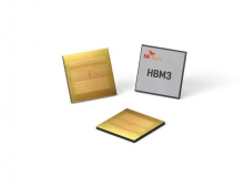
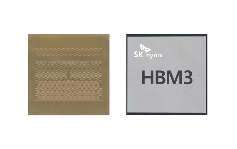
“With continued advancements in HPC and AI applications, demands for higher performance and improved power efficiency has been growing more than ever before. With the current release of the HBM3 JEDEC standard, SK hynix is pleased to be able to provide a memory to our customers that has the highest bandwidth and the best power efficiency existing today with added robustness through adoption of an enhanced ECC scheme. SK Hynix is proud to be part of JEDEC and is thereby excited to be able to continue to build a strong HBM eco-system together with our industry partners, and to provide both ESG and TCO values to our customers”, said Uksong Kang, Vice President of DRAM Product Planning at SK hynix.
“Synopsys has been an active contributor of JEDEC for more than a decade, helping to drive development and adoption of the most advanced memory interfaces like HBM3, DDR5 and LPDDR5 for a range of emerging applications,” said John Koeter, Senior Vice President of Marketing and Strategy for IP at Synopsys. “The Synopsys HBM3 IP and verification solutions, already adopted by leading customers, accelerate the integration of this new interface into high-performance SoCs and enable development of multi-die system-in-package designs with maximum memory bandwidth and power-efficiency.”