Nikon To Release 450mm Immersion Scanner in 2017
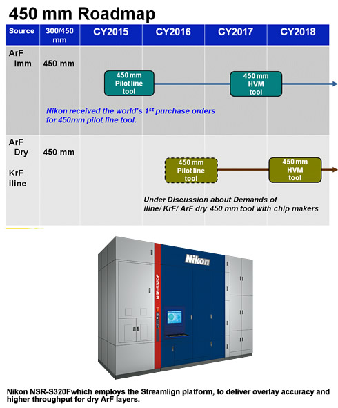
Nikon had entered into a contract with the Research Foundation for the State University of New York (Research Foundation for SUNY) to provide a 450mm wafer ArF immersion scanner for process development and to be entrusted with wafer patterning subsequently received an order for the system.
Scheduled to be shipped in April 2015, the 450mm wafer ArF immersion scanner will be used by the member companies of the Global 450 Consortium (G450C) headquartered in the College of Nanoscale Science and Engineering (CNSE) for process development, characterization and demonstrations. Nikon will provide lithography solutions by sending its engineers to G450C. Nikon aims for the standardization of 450mm wafer ArF immersion scanners by offering early opportunities to develop 450mm process.
Announced by New York Governor Andrew M. Cuomo in September 2011 and located in the Albany NanoTech Complex at CNSE, G450C is a joint effort by Intel, IBM, GLOBALFOUNDRIES, TSMC and Samsung, involved in the next generation of computer chip technologies.

The goal of G450C is to support the industry transition from 300mm to the 450mm wafer platform, a crucial tipping point for the semiconductor manufacturing process, as smooth as possible. G450C plans to build advanced infrastructure in the Albany NanoTech Complex to demonstrate the capabilities of 450mm wafer platform and process.
Nikon expects to see increased orders for its systems from other device manufacturers in time for shipments of high volume manufacturing systems scheduled in 2017.
IC Insights research firm expects that 450mm wafer capacity will account for just one-tenth of a percent of global IC capacity in December 2017.
Announced by New York Governor Andrew M. Cuomo in September 2011 and located in the Albany NanoTech Complex at CNSE, G450C is a joint effort by Intel, IBM, GLOBALFOUNDRIES, TSMC and Samsung, involved in the next generation of computer chip technologies.

The goal of G450C is to support the industry transition from 300mm to the 450mm wafer platform, a crucial tipping point for the semiconductor manufacturing process, as smooth as possible. G450C plans to build advanced infrastructure in the Albany NanoTech Complex to demonstrate the capabilities of 450mm wafer platform and process.
Nikon expects to see increased orders for its systems from other device manufacturers in time for shipments of high volume manufacturing systems scheduled in 2017.
IC Insights research firm expects that 450mm wafer capacity will account for just one-tenth of a percent of global IC capacity in December 2017.


