QLC NAND Flash to Succeed TLC NAND Next Year
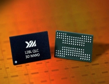
Samsung's 4bit/cell flash is on the way and according to the company, the QLC (quad-level cell) NAND chip will contain more information at a lower price.
"QLC NAND flashes are not yet in mass-production, but we are preparing it internally," an official at Samsung Electronics told Business Korea. "QLC NAND flashes can store four times as much data as SLC NAND flashes."
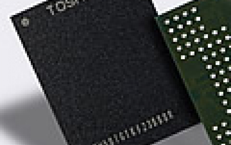
Other NAND flash makers such as Toshiba and SK Hynix are also reportedly preparing for QLC NAND flash production.
The highest capacity flash cells right now are TLC (triple-level cell) with 3 bits/cell. QLC NAND flash stores four bits of data in one cell. But it's harder to make QLC flash as it has slower read and write times than TLC and less endurance at die level.
In order to put a lot of data into one cell, the process must be finer. An SLC NAND flash requires two gates that can distinguish between 1 and 0 in one cell but an MLC NAND flash and a TLC NAND flash needs to be segmented to have four and eight gates.
This also increases difficulties in development and manufacturing. However, more data can be stored on wafers of the same size, which can significantly mark down prices.
According to IHS Markit, TLC NAND flashes accounted for 65% of the global NAND flash market as of the end of the third quarter, exceeding multi-level cell (MLC) NAND flashes (37.5%). Given the fact that TLC NAND flashes and MLC NAND flashes accounted for 56.1% and 43.6% of the market, respectively, at the end of 2016, the market has been shifting rapidly toward TLC NAND flashes this year.
QLC flash should arrive in the first 2018 quarter, according to IHS Markit.
3D NAND Scaling issues
At the Flash Memory Summit this year, Samsung announced its development of 1Tb 3D NAND, which would be used for commercial products launching next year.
Based on the information available on TLC 512Gb 3D NAND with 64-layer on about 130mm2 die size and assuming string stacking of 64-layer.
According to Sang-Yun Lee, CEO of BeSang Inc. BeSang Inc., it will be very difficult to further expand 3D NAND's memory scaling in a vertical direction. For example, in order to implement a much larger 4Tb NAND chip 8 string stacks of 64-layer are needed. The total layer would become 512-layer on 130mm2 die size, which
will take about a year to process a wafer, plus many more weeks for memory logic and a 64-layer cell layer implementation. Therefore, the wafer processing time for a 512-layer will be about 45 to 53 weeks (!).
This would make practically impossible to implement the 4Tb NAND chip. If QLC is considered instead of TLC, there will be an improvement of 25 percent at best. So, a 410-layer will be needed for QLC 4Tb 3D NAND and about nine months (!) of wafer processing time.
Will 3D NAND reach the end of its life span soon?


