UMC Produces Working 45nm ICs
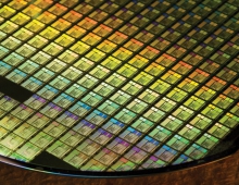
Taiwanese UMC has successfully produced functional 45-nanometer (nm) SRAM chips that feature a bit cell size of less than 0.25΅m2.
The ICs, produced using UMC's independently developed logic process, used immersion lithography for its 12 critical layers and incorporated the latest technology advancements such as ultra shallow junction, mobility enhancement techniques, and ultra low-Κ dielectrics (Κ=2.5).
The 45nm SRAM memory bit-cell and macro circuit require good minimum supply voltage capability, which is an important aspect for 45nm, due to the demanding power saving requirements of today's advanced portable electronics. In addition, by using optional circuits built into the test vehicle, the minimum supply voltage level can be further improved to achieve excellent power behavior.
Producing working SRAM is a key first-step in demonstrating technology performance and process reliability prior to engaging customers for the manufacturing of their 45nm products. UMC's 45nm process features a 30% design rule shrink, 50% 6-transistor SRAM cell size shrink, and a 30% device performance gain over the 65nm technology node, which is in production at UMC for several customer products. Development for UMC's 45nm process is taking place at the foundry's 300mm Fab 12A, located in Tainan Science Park in southern Taiwan


