
Toshiba Develops a New High-k/Ge Gate Stack Technology for LSIs at 16nm Node and Beyond
Toshiba today announced a significant advance in the development of a gate stack and interlayer with high carrier mobility that can be applied to advanced metal-insulator-semiconductor field-effect transistors (MISFETs) in future generations of LSIs.
The ultra-thin, Equivalent Oxide Thickness (EOT) -scalable high-k/Ge gate stack with strontium germanide (SrGex ) interlayer with high carrier mobility is a basic technology with potential for application in MISFETs at the 16 nm node and beyond. The technology will be presented today during Session 4B of the 2009 VLSI Symposia in Kyoto, Japan.
Current MISFET uses silicon for the channel, but physical limitations of silicon will make it difficult to obtain sufficient drive current in future scaled down MISFETs. Germanium (Ge) has long been known as an alternative offering higher carrier mobility characteristics, but significant technical challenges exist in implementing germanium in LSIs. Development of gate stack structures for Ge-MISFETs is one of the challenges. There are reports of achieving high hole mobility by adopting germanium dioxide (GeO2 ) in the gate stack insulating layer, but due to its low dielectric constant, there still remains the challenge of reducing the EOT to 0.5 nm, which is required for the 16 nm node and after.
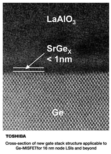
Toshiba has achieved a technology that overcomes the twin challenges of fabricating a thin gate stack while maintaining high hole mobility, by inserting SrGex , a compound of strontium (Sr) and germanium, as an interlayer between the high-k insulating layer and the germanium channel.
Germanium is first subject to heat surface treatment in an ultra-high vacuum, and a layer of strontium of up to ten atoms is deposited on the surface of the germanium, followed by a lanthanum aluminate (LaAlO3 ) high-k film. Finally, the gate stack is annealed in a nitrogen atmosphere. The SrGex layer is formed during these processes, between the high-k film and the germanium channel.
The new technology realizes peak hole mobility of 481 cm2 /Volt second (Vsec), a record high value for high-k/Ge p-MISFETs. This value is over three times than that obtained without the SrGex interlayer, and over twice the universal mobility that can be realized with silicon (based on comparison with the same gate field).
Toshiba also confirmed that a gate stack structure with EOT as thin as around 1 nm was successfully formed, and that the increase in EOT by inserting the SrGex interlayer was only 0.2 nm at the most. This suggests the possibility of further EOT scaling to 0.5 nm, either by reducing thickness of an overlaying high-k layer or adopting a high-k layer with a higher dielectric constant.
Toshiba will continue to develop the technology as an option toward implementation of Ge-MISFET to 16 nm LSIs and beyond.
Development of this new gate stack process technology was supported by grants from Japan's New Energy and Industrial Technology Development Organization (NEDO).
Current MISFET uses silicon for the channel, but physical limitations of silicon will make it difficult to obtain sufficient drive current in future scaled down MISFETs. Germanium (Ge) has long been known as an alternative offering higher carrier mobility characteristics, but significant technical challenges exist in implementing germanium in LSIs. Development of gate stack structures for Ge-MISFETs is one of the challenges. There are reports of achieving high hole mobility by adopting germanium dioxide (GeO2 ) in the gate stack insulating layer, but due to its low dielectric constant, there still remains the challenge of reducing the EOT to 0.5 nm, which is required for the 16 nm node and after.
Toshiba has achieved a technology that overcomes the twin challenges of fabricating a thin gate stack while maintaining high hole mobility, by inserting SrGex , a compound of strontium (Sr) and germanium, as an interlayer between the high-k insulating layer and the germanium channel.
Germanium is first subject to heat surface treatment in an ultra-high vacuum, and a layer of strontium of up to ten atoms is deposited on the surface of the germanium, followed by a lanthanum aluminate (LaAlO3 ) high-k film. Finally, the gate stack is annealed in a nitrogen atmosphere. The SrGex layer is formed during these processes, between the high-k film and the germanium channel.
The new technology realizes peak hole mobility of 481 cm2 /Volt second (Vsec), a record high value for high-k/Ge p-MISFETs. This value is over three times than that obtained without the SrGex interlayer, and over twice the universal mobility that can be realized with silicon (based on comparison with the same gate field).
Toshiba also confirmed that a gate stack structure with EOT as thin as around 1 nm was successfully formed, and that the increase in EOT by inserting the SrGex interlayer was only 0.2 nm at the most. This suggests the possibility of further EOT scaling to 0.5 nm, either by reducing thickness of an overlaying high-k layer or adopting a high-k layer with a higher dielectric constant.
Toshiba will continue to develop the technology as an option toward implementation of Ge-MISFET to 16 nm LSIs and beyond.
Development of this new gate stack process technology was supported by grants from Japan's New Energy and Industrial Technology Development Organization (NEDO).