Intel, Samsung Provide EUV Progress Updates At SPIE
SPIE's 2017 Advanced Lithography Conference kicked off in San Jose, California and respesentatives from Intel and Samsung said that Extreme ultraviolet (EUV is making significant progress, although hurdles remain.
Last October, Samsung announced plans announced to use EUV for its 7nm node, but it has yet to say how and when. Intel remains more sceptical, remaining loayal to its previous plan that it will use EUV
only be used when it is ready.
Intel's Britt Turkot leads the company's EUV program and presented
eight core EUV programs currently ready, including a pellicle covering for EUV wafers currently in development, and a new tool for inspecting EUV masks.
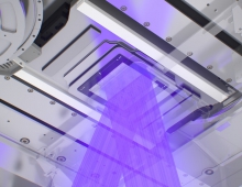
Samsung described an EUV mask inspection tool suitable for 7nm that it has been developing in house. Turkot said the lack of such tools from third parties would not prevent use of EUV but could reduce yields and increase costs.
Late last year Samsung produced its first EUV masks with five or fewer defects, a level making them suitable for repair.
With ever-smaller feature sizes being designed, from 22nm to 10nm, with features 1/10 the size of the wavelength of the exposure tool, mask makers continuously advance resolution and reduce defects.
Dr. Frank Abboud, Vice President Technology Manufacturing Group and General Manager, Intel Mask Operation, noted that photomasks act as diffractive optical elements in the lithography process: they modify all parameters of impingent light including intensity, direction, phase, and polarization. Extreme Ultraviolet (EUV) sources are, in Abbouds words, "More disruptive to the mask shop than the wafer fab. Almost every module in the mask shop is touched", including blank preparation, fiducial mark patterning, device patterning, black-border patterning, and metrology/characterization.
Looking ahead to answer the question of whether mask makers are ready for EUV, Abboud described the Intel Mask Operation approach to adopting EUV lithography through supply chain development, consortia, collaboration, co-development and internal programs. The results include full field EUV pellicles demonstrated in 2014 and product reticles shipped in 2016. There have been continuous improvements with champion results reported as 2 defects at 38nm scale, which allows one to map the defects, move and cover the defects, and thus avoid the defects in practice. Abboud noted how electron-beam technology is being adopted in EUV mask defect repairs.
Over time, more of the photomask work is done at internal (captive) mask shops like at Intel, with VLSI predicting mask volume will decrease 10%, but cost will increase 30% over the next few years, primarily driven by the capital spending necessary to shift to EUV. However, Abboud assured the SPIE plenary audience that, "The next technology paradigm -- EUV -- will not be gated by mask."
Intel shipped to its wafer fab its first product-quality EUV masks last year. Its EUV mask pilot line has created multiple defect-free EUV reticles at 14, 10 and 7nm, said Turkot.
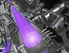
Another serious hurdle in the EUV lithography process is the performance and reliability of the EUV equipment. Both Intel and Samsung experts agreed EUV source power has made significant strides toward a 250W target. However, there is still a gap between the 210W lab demonstration EUV maker ASML reported late last year and the 130W performance of the best systems in the field. Turkot said that
the lifetimes of droplet generators and collectors in the light source has lengthened and become more predictable. Overall EUV uptimes are improving but not fast enough, she said.
The latest ASML 3350B systems were available more than 75 percent of the time by the end of last year, up about five percent from the prior year's results.
Turkot expressed optimism that pellicles to keep defects off EUV wafers are progressing with new pilot films ramping and production films in development. Samsung's Kim said new pellicle materials are needed to withstand 250W production scanners.
Photoresist materials are hitting performance targets for 7nm but need greater sensitivity for production use. The chemicals will not be a limiter for using EUV but could be in the future if advances cannot handle line-edge roughness and edge placement, Turkot said.
Currently, 14 EUV systems are now in use worldwide, and six of them are 3350Bs, Turkot added.

