Breaking News

ADATA and MSI Launch the World’s First 4-RANK DDR5 CUDIMM Memory Module Akasa Introduces Kepler: A 2U Rackmount Fanless Case Designed for Silent Computing in Industrial Applications LIAN LI Introduces the Platinum Certified SX PSU Series Micron Ships Automotive UFS 4.1 Apple introduces Digital ID

logo

  • Share Us
    • Facebook
    • Twitter
  • Home
  • Home
  • News
  • Reviews
  • Essays
  • Forum
  • Legacy
  • About
    • Submit News

    • Contact Us
    • Privacy

    • Promotion
    • Advertise

    • RSS Feed
    • Site Map

Search form

Samsung to Produce Its Own 1,000fps, 3-layer Image Sensor for Smartphones

Samsung to Produce Its Own 1,000fps, 3-layer Image Sensor for Smartphones

Smartphones Sep 18,2017 0

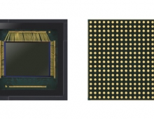
Samsung has developed and plans to mass produce a 3-layer CMOS image sensor for smartphones, which can shoot slow-motion video at a 1,000 frames per second.

The concept is familiar for those watching the CMOS market, as Sony has already released 3-layer sensors for smarthones and its premium Xperia XZ and XZ1 models: the CMOS has a stacked configuration with a back-illuminated pixel array, a signal processing circuit layer and DRAM. The DRAM used in Sony's sensor is from Micron.

Samsung's CMOS will also have a layered structure - sensor, a logic chip along with Samsung's DRAM memory - using the through-silicon via (TSV) interconnect technique.

Samsung has already ordered the equipment required in order to mass produce the new sensor and plans to start mass production by November.

Image sensors typidally used in current premium Smartphones are based on a 2-layered structure that is composed of a sensor and a logic chip. The image processing required for detecting and tracking of objects has to be carried out at a later stage.

Sony's CMOS features a Micron's DRAM chip placed between an image sensor and a logic chip. The Japanese company has developed a batch process system that attaches a sensor, a DRAM chip, and a logic chip in a single wafer. Samsung's approach will be to use first create a 2-layered structure with a sensor and a logic chip and then attach the DRAM memory using a Thermocompression bonding approach. It is a wafer bonding technique in which two metals are brought into atomic contact applying force and heat simultaneously. The diffusion requires atomic contact between the surfaces due to the atomic motion. The atoms migrate from one crystal lattice to the other one based on crystal lattice vibration. This atomic interaction sticks the interface together.

Obviously, Sony's approach is more productive and cost-efficient, but Samsung has obviously decided to use the TC approach in order to avoid possible patent infringments. On the other hand, Samsung has an advantage over Sony as it will receive the DRAM chips internally.

It is predicted that Samsung's new 3-layered image sensors will be used in the company's next Galaxy Smartphones. Currently, Samsung receives half of the required image sensors from Sony and the other half from its own Semiconductor Business Department.

Tags: CMOS image sensor
Previous Post
Free CCleaner Software Compromised to Open Back-door to Million of PCs
Next Post
Google Introduces the Tez Mobile Payments and Commerce App in India

Related Posts

  • Samsung Introduces 1.2μm 50Mp ISOCELL GN1 With Faster Auto-focusing and Brighter Images

  • Sony to Release Intelligent Vision Sensors with AI Processing Built in

  • Sony's SWIR Image Sensors Capturing Images Across Both the Visible and Invisible Light Spectrums

  • OmniVision Unveils First 0.7 Micron, 64 Megapixel Image Sensor for High End Smartphones

  • SK hynix’s Black Pearl 1.0um and 0.8um Image Sensors Launching This Year

  • OmniVision Announces Its First 64 Megapixel, 0.8 Micron Image Sensor For Smartphones

  • Samsung’s 108Mp ISOCELL Bright HM1 Promises Brighter Ultra-High-Res Images With Nonacell Technology

  • Samsung Explains How Its ISOCELL Bright HMX 108MP Image Sensor Works

Latest News

ADATA and MSI Launch the World’s First 4-RANK DDR5 CUDIMM Memory Module
PC components

ADATA and MSI Launch the World’s First 4-RANK DDR5 CUDIMM Memory Module

Akasa Introduces Kepler: A 2U Rackmount Fanless Case Designed for Silent Computing in Industrial Applications
Cooling Systems

Akasa Introduces Kepler: A 2U Rackmount Fanless Case Designed for Silent Computing in Industrial Applications

LIAN LI Introduces the Platinum Certified SX PSU Series
PC components

LIAN LI Introduces the Platinum Certified SX PSU Series

Micron Ships Automotive UFS 4.1
Enterprise & IT

Micron Ships Automotive UFS 4.1

Apple introduces Digital ID
Enterprise & IT

Apple introduces Digital ID

Popular Reviews

be quiet! Dark Mount Keyboard

be quiet! Dark Mount Keyboard

Terramaster F8-SSD

Terramaster F8-SSD

be quiet! Light Mount Keyboard

be quiet! Light Mount Keyboard

Soundpeats Pop Clip

Soundpeats Pop Clip

Akaso 360 Action camera

Akaso 360 Action camera

Dragon Touch Digital Calendar

Dragon Touch Digital Calendar

Noctua NF-A12x25 G2 fans

Noctua NF-A12x25 G2 fans

be quiet! Pure Loop 3 280mm

be quiet! Pure Loop 3 280mm

Main menu

  • Home
  • News
  • Reviews
  • Essays
  • Forum
  • Legacy
  • About
    • Submit News

    • Contact Us
    • Privacy

    • Promotion
    • Advertise

    • RSS Feed
    • Site Map
  • About
  • Privacy
  • Contact Us
  • Promotional Opportunities @ CdrInfo.com
  • Advertise on out site
  • Submit your News to our site
  • RSS Feed