Globalfoundries Says 22nm eMRAM Could Displace eFlash
Globalfoundries is promoting its eMRAM technology as a potential high-volume embedded flash (eFlash) replacement.
GF’s 22nm FD-SOI (22FDX) embedded MRAM non-volatile memory (NVM) technology, which has entered pilot production for the company's large IoT clients.
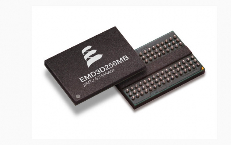
The embedded STT-MRAM (spin-transfer torque magnetoresistive RAM) technology, developed by GF partnership with Everspin Technologies, Inc., is aimed at IoT, general-purpose microcontrollers, automotive, edge AI and other applications where low-power operation and non-volatile code and data storage is a critical requirement.
GF says that its eMRAM technology has passed real-world production testing, and enables delivery of persistent data retention and endurance at extended temperatures. That is key for microcontroller applications and wireless connected IoT, where embedded memory must retain code and data at high temperatures, including through solder reflow at 260°C during PCB assembly. It also offers erase and (re)write speeds an order of magnitude faster than eFlash (200 nanoseconds vs. 10’s of microseconds), with comparable read speeds, providing a power advantage over eFlash in many applications.

Although it initially makes use of GF’s 22FDX process, MRAM is deployed in ‘back-end-of-line’ metallization, which allows for a roadmap with planned derivatives on both FDX and GF’s FinFET technology. That’s because STT-MRAM as a memory technology allows for process variations which can be used to tune the memory bit cell. Accordingly, Globalfoundries expects to offer two “flavors” of eMRAM: eMRAM-F on 22FDX for code/data storage right now, and eMRAM-S as a working memory to augment SRAM at 1x nodes in the future.
GF is currently running multi-project wafers (MPWs) with 22FDX-based eMRAM-F designs for several clients, and multiple production tape-outs are scheduled in the next three quarters. Custom design services are available from GF and the company's design partners, and 22FDX eMRAM process design kits are available with macro densities ranging from 4Mb to 32Mb for individual macros. A 48Mb macro is scheduled for release in 4Q19 as well.
Many new eNVM memory technologies look interesting but aren’t yet production-ready. For example, RRAM (resistive RAM), which stores data by changing the electrical resistance of a dielectric, is the subject of much research and development but its maturity on 2x nm process nodes is limiting its adoption. Likewise adoption for PCM memory is limited by a lack of foundry support below 28nm.


