Globalfoundries Offers Post-Fab Turnkey Services As 5G Arrives
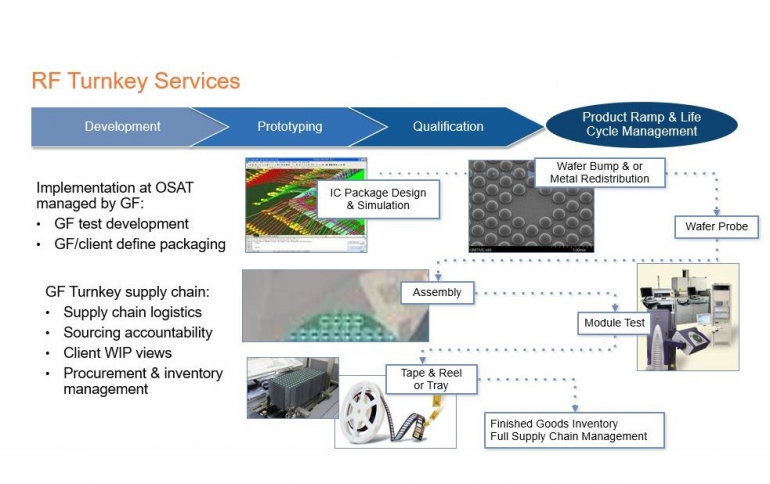
In addition to a portfolio of RF platforms for wafer fabrication, chip maker GLOBALFOUNDRIES (GF) offers clients expertise in an array of post-fab turnkey services – along every step of the way, from finished wafer to tape-and-reel.
Post-fab assembly, test, and advanced packaging functions are critical to the successful production of RF/mmWave integrated circuits (ICs) because the physics at these frequencies is complex, which makes it extremely difficult to accurately characterize and test these devices.
GF offers post-fab turnkey services to clients of all sizes who may have very different business models. The two extremes are startups focused primarily on product design and have very little capability in resourcing post-fab functions, and larger companies who also are focused on design but may not have the expertise or capability in complex post-fab activities for RF/mmWave.
GF’s services are based on in-house RF expertise and include proprietary RF/mmWave testing technology, flexible engagement models to fit a client’s particular needs, and expert supply chain management.
In particular, GF’s in-house RF/mmWave test capability, called tester-on-board (ToB), represents a new testing paradigm for mmWave ICs. Traditional high-volume manufacturing test equipment is unable to cost-effectively perform the required testing of mmWave ICs in production environments – including, for example, measuring linearity and output power, verifying phase shifter performance, and validating noise figures. GF says that its ToB solution, a modular plug-and-play system based on technology developed at IBM that reduces the cost of testing by 3-5 times versus rack-and-stack systems.
The increased complexity that comes with 5G mmWave applications calls for a unified design/production approach, taking into account front- and back-end considerations holistically in order to get the desired performance and reliability from a mmWave IC.
Packaging is a critical component in determining the performance of mmWave devices, said Peter Rabbeni, GF’s vice president of Mobile and Wireless Infrastructure. If packaging is regarded just as a back-end function, he said, clients may get bogged down in post-fab complexities, which could require additional time and, in turn, potentially result in missing a window of opportunity in the market.
“It’s not sufficient to simply test product performance at the wafer level at these frequencies. The specifications must be met in actual over-the-air operation through finished, packaged products,” he said. GF’s expertise with RF technologies and the company’s unique in-house RF testing capabilities are powerful tools that help clients meet this requirement. Rabbeni gave as an example a typical challenge faced by 5G base station designers: how to optimally design the power amplifier (PA) in a base station to balance reliability and achievable output power so that a handset can pick up its transmitted signal.
“Signal strength is key, of course, but there are modulation peaks and valleys that make it hard to know exactly how hard to drive the PA,” Rabbeni said. “Drive the PA too hard and you not only compromise signal quality but also PA lifetime. Drive the PA too weak and you leave efficiency on the table. There’s a ‘sweet spot’ that balances optimum power and reliability for optimum coverage. This also helps optimize the number of base stations needed to get the required coverage,” and ultimately minimizes operator capital expenditures and operating expenses, he said.
“The key to determining this sweet spot quickly and cost-effectively is having the ability to accurately simulate the performance of the PA and to characterize its reliability under any set of modulation conditions,” Rabbeni said. “GF’s process design kits incorporate our extensive RF intellectual property for device reliability and performance modeling and enable clients to perform these simulations quickly and easily.”
Beyond 5G, GF’s post-fab turnkey services are likely to become even more important in the years to come. Guido Uberreiter, GF’s vice president of Tapeout, Mask and Postfab Operations, sees a future where RF/mmWave capabilities increasingly are added to state-of-the-art logic chips for AI, cloud computing, automotive, and other applications.
“As you look to the future you see an increasing number of applications that have to do with AI and cloud computing. This next wave of clients – many of which will be small and mid-sized companies – will want to combine RF with logic for such things as automotive radar, and they will need to find a solution to build RF SoCs (system-on-chip) in a way that is both the most cost-effective and very fast,” he said.
“They don’t want to have to send chips around the world many times, and this plays exactly to our strengths. In Dresden, for example, we have a center of excellence for bump-and-test, until now essentially dedicated to logic chips, given our 20-year history of producing advanced logic ICs in Dresden for clients. Today, we take the output from GF Fab 1 in Dresden, and Fab 8 in Malta, then bump, test, and send the tested wafers to clients. We will evolve these services to include the specialized RF expertise, and deliver them in an exceptional way for the 40-80 GHz range,” he said.


