IBM-Led Chip Alliance Delivers Semiconductor Performance Leap Using "High-K/Metal Gate" Material
IBM and its joint development partners today announced that they have collectively demonstrated significant performance and power consumption advantages over industry standards by using a new material known as "high-k/metal gate" (HKMG) on silicon.
IBM's partners include Chartered Semiconductor Manufacturing Ltd., Freescale Inc., Infineon Technologies AG, Samsung Electronics Co., Ltd., STMicroelectronics N.V. and Toshiba Corporation.
Significant performance and power improvements have been observed in HKMG evaluation circuits and test chips on silicon manufactured at IBM's East Fishkill, N.Y. semiconductor fabrication facility. The alliance has assessed performance improvements on 32nm technology circuits of up to 35 percent over 45nm technology circuits at the same operating voltage. The 32nm power reduction over 45nm can be as much as 30 to 50 percent depending on the operating voltage. In addition, testing on product library test chip and industry standard microprocessor critical paths has shown performance improvements of up to 40 percent over conventional (Poly/SiON) technology at the same technology dimensions.
 "These early high-k/metal gate results demonstrate that by working together we can deliver leading-edge technologies that handily surpass others in the industry," said Gary Patton, vice president for IBM's Semiconductor Research and Development Center on behalf of the technology alliance. "Demonstrating this caliber of result in a practical environment means that as our collective client base moves to next-generation technology by using the 'gate-first' approach, they will continue to maintain a significant competitive advantage."
The Common Platform alliance partners ? IBM, Chartered and Samsung ? are the first in the original equipment manufacturing (OEM) foundry industry to unveil a HKMG technology in the 32nm technology generation. A low-power 32nm technology design enablement package with compatible ground rules for extendibility to the 28nm technology generation is now available. Silicon support for low-power 32nm HKMG technology will be available through a prototyping shuttle program starting in the third quarter of 2008, with plans for quarterly shuttles. Feasibility results from HKMG devices built at the College of Nanoscale Science and Engineering?s Albany NanoTech Complex indicate this process can be extended to 22nm, demonstrating that improvements resulting from the use of HKMG can continue to be delivered in successive technology generations.
"This early design and modeling work indicates that the high-k/metal gate technology is going to deliver a significant product and performance differentiation. These early results are a significant step in the demonstration of high-k/metal gate viability in 32nm technology," said Dirk Wrister, director of Process Technology at Freescale.
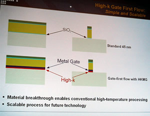
On January 29, 2007, IBM and its research partners (including Sony and Toshiba) introduced the high-k/metal gate innovation as the basis for a long-sought improvement to the transistor ? the tiny on/off switch that serves as the basic building block of virtually all microchips made today. Using the high-k/metal gate material in a critical portion of the transistor that controls its primary on/off switching function enabled the development of 32nm chip circuitry that is designed to be smaller, faster, and more power-efficient than previously thought possible.
Significant performance and power improvements have been observed in HKMG evaluation circuits and test chips on silicon manufactured at IBM's East Fishkill, N.Y. semiconductor fabrication facility. The alliance has assessed performance improvements on 32nm technology circuits of up to 35 percent over 45nm technology circuits at the same operating voltage. The 32nm power reduction over 45nm can be as much as 30 to 50 percent depending on the operating voltage. In addition, testing on product library test chip and industry standard microprocessor critical paths has shown performance improvements of up to 40 percent over conventional (Poly/SiON) technology at the same technology dimensions.
 "These early high-k/metal gate results demonstrate that by working together we can deliver leading-edge technologies that handily surpass others in the industry," said Gary Patton, vice president for IBM's Semiconductor Research and Development Center on behalf of the technology alliance. "Demonstrating this caliber of result in a practical environment means that as our collective client base moves to next-generation technology by using the 'gate-first' approach, they will continue to maintain a significant competitive advantage."
The Common Platform alliance partners ? IBM, Chartered and Samsung ? are the first in the original equipment manufacturing (OEM) foundry industry to unveil a HKMG technology in the 32nm technology generation. A low-power 32nm technology design enablement package with compatible ground rules for extendibility to the 28nm technology generation is now available. Silicon support for low-power 32nm HKMG technology will be available through a prototyping shuttle program starting in the third quarter of 2008, with plans for quarterly shuttles. Feasibility results from HKMG devices built at the College of Nanoscale Science and Engineering?s Albany NanoTech Complex indicate this process can be extended to 22nm, demonstrating that improvements resulting from the use of HKMG can continue to be delivered in successive technology generations.
"This early design and modeling work indicates that the high-k/metal gate technology is going to deliver a significant product and performance differentiation. These early results are a significant step in the demonstration of high-k/metal gate viability in 32nm technology," said Dirk Wrister, director of Process Technology at Freescale.
On January 29, 2007, IBM and its research partners (including Sony and Toshiba) introduced the high-k/metal gate innovation as the basis for a long-sought improvement to the transistor ? the tiny on/off switch that serves as the basic building block of virtually all microchips made today. Using the high-k/metal gate material in a critical portion of the transistor that controls its primary on/off switching function enabled the development of 32nm chip circuitry that is designed to be smaller, faster, and more power-efficient than previously thought possible.


