Intel’s Embedded Multi-Die Interconnect Bridge Helps Chips ‘Communicate’ Faster
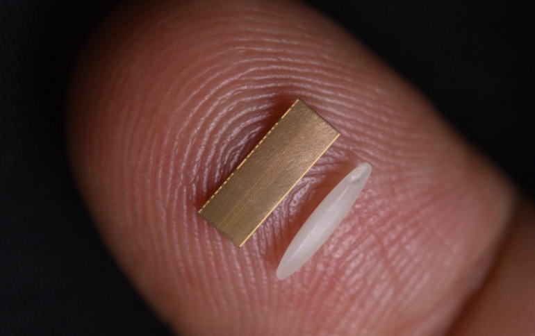
An Intel technology called EMIB (embedded multi-die interconnect bridge) is a complex multi-layered sliver of silicon no bigger than a grain of rice, which lets chips fling enormous quantities of data back and forth among adjoining chips at blinding speeds: several gigabytes per second.
Most chips in today’s smartphones, computers and servers are comprised of multiple smaller chips invisibly sealed inside one rectangular package.
These multiple chips — often including CPU, graphics, memory, IO and more — can communicate using Intel EMIBs, which speed the flow of data inside nearly 1 million laptops and field programmable gate array devices worldwide.
Intel expects that number to soon soar and include more products as EMIB technology enters the mainstream. For example, Intel’s Ponte Vecchio processor, a general-purpose GPU the company unveiled Nov. 17, contains EMIB silicon.
This technology allows chip architects to cobble together specialized chips faster. And compared with an older, competing design called an interposer — in which chips inside a package sit atop what is essentially a single electronic baseboard, with each chip plugged into it — tiny, flexible, cost-effective EMIB silicon offers an 85% increase in bandwidth. That can make your tech — laptop, server, 5G processor, graphics card— run dramatically faster.
The industry refers to this application as 2.5D package integration. Instead of using a large silicon interposer typically found in other 2.5D approaches, EMIB uses a very small bridge die, with multiple routing layers. This bridge die is embedded as part of our substrate fabrication process.
Traditional solutions to this challenge are categorized as 2.5D solutions, utilizing a silicon interposer and Through Silicon Vias (TSVs) to connect die at so-called silicon interconnect speed in a minimal footprint. The result is increasingly complex layouts and manufacturing techniques that delay tape-outs and depress yield rates.
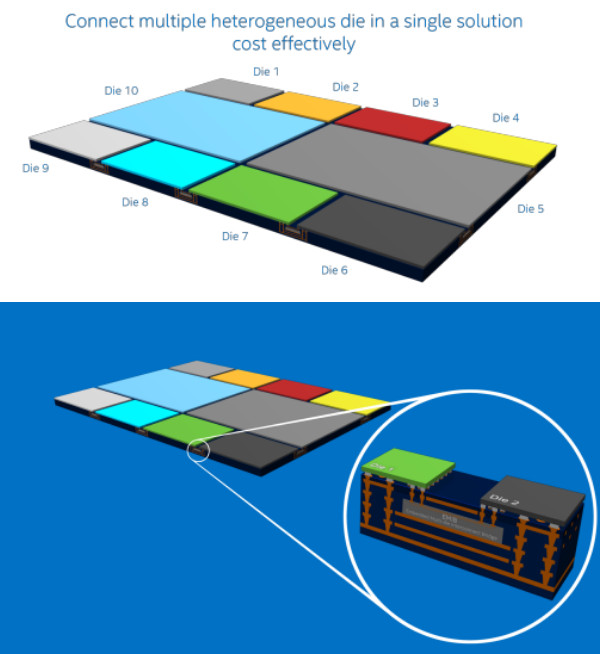
Intel sought a solution that is practical to design, reliable across any die, and simple to implement in a design. The result is EMIB. There can be many embedded bridges in a single substrate, providing extremely high I/O and well controlled electrical interconnect paths between multiple die, as needed. Because the chips do not have to be connected to the package through a silicon interposer with TSVs, there is nothing to potentially degrade their performance. Intel uses micro-bumps for high density signals, and coarser pitch, standard flip chip bumps for direct power and ground connections from chip to package.
The cross-section shows two die that have been assembled to a package with micro-bumps providing die-to-die connections through a bridge chip.
The silicon interposer in a typical 2.5D package is a piece of silicon larger-than-all interconnecting die. In contrast, the silicon bridge is a small piece of silicon embedded only under the edges of two interconnecting die. This allows for most size die to be attached in multiple dimensions, eliminating additional physical constraints on heterogeneous die attachment within the theoretical limits.
Intel promises that the next-generation EMIB could double or even triple that bandwidth.

