Intel Demonstrates First Co-Packaged Optics Ethernet Switch
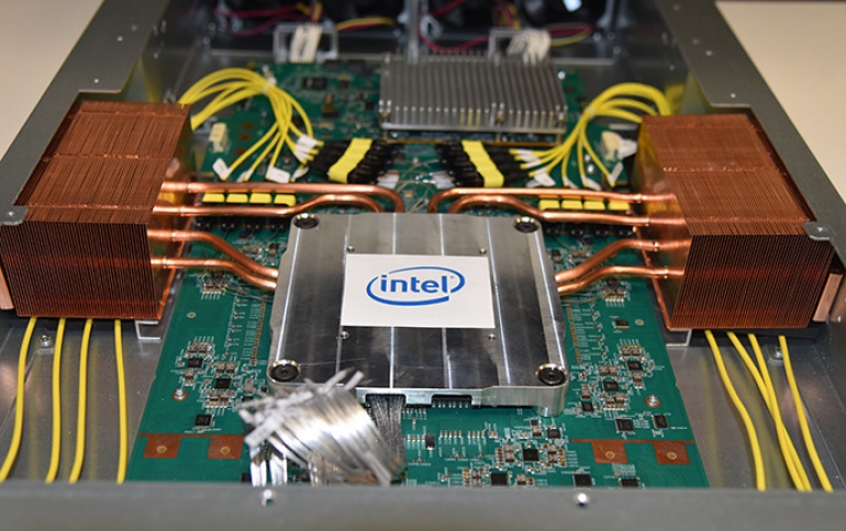
Intel has successfully integrated its 1.6 Tbps silicon photonics engine with its 12.8 Tbps programmable Ethernet switch. This co-packaged solution brings together the essential technology building blocks from Intel and its Barefoot Networks Division for integrated optics on an Ethernet switch.
“Our co-packaged optics demonstration is the first step to making optical I/O with silicon photonics a reality. We share the industry belief that co-packaged optics offers power and density advantages for switches at 25 Tbps and higher, and ultimately is a necessary and enabling technology for bandwidth scalability in future networks. The timing of this demonstration shows the technology is ready to support our customers’ requirements.”
–Hong Hou, Intel corporate vice president and general manager of the Silicon Photonics Products Division
The co-packaged switch is optimized for hyperscale data centers, where demand for cost-effective interconnect and bandwidth is limitless. Intel is currently demonstrating this technology to its customers.
Today’s data center switches depend on pluggable optics installed in the switch faceplate that are connected to switch serializer/deserializer (SerDes) ports using an electrical trace. But as data center switch bandwidth grows, connecting the SerDes to pluggable optics electrically will be more complex and require more power. With co-packaged optics, the optical port is placed near the switch within the same package, thus reducing power and enabling continued switch bandwidth scalability.
Intel's demonstration brings together the best of Barefoot Networks’ programmable Ethernet switch technology and Intel’s silicon photonics technology. The integrated switch package in this demonstration uses a P4-programmable Barefoot Tofino 2 switch ASIC co-packaged with 1.6 Tbps silicon photonics engines from Intel’s Silicon Photonics Product Division.
Barefoot Tofino 2 is a P4-programmable Ethernet switch that delivers up to 12.8 Tbps throughput and is based on the company’s Protocol Independent Switch Architecture (PISA). PISA is programmed using the open source P4 programming language for data planes. With the P4 data plane, Tofino switches’ forwarding capability can be adapted via software to new needs in the network or to new protocols that are supported by P4. The performance and programmability of Tofino 2 are designed to meet the needs of hyperscale data centers and cloud and service provider networks.
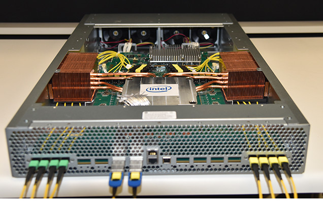
For co-packaged optics, the Barefoot Tofino 2 switch ships in a multi-die package that makes it easier to co-package the optical engine and to upgrade the SerDes for lower power or higher throughput.
The silicon photonics interconnect platform features 1.6 Tbps photonic engines realized as 4 ports of 400GBase-DR4 interfaces, designed and manufactured in the Intel silicon photonics platform. The engines are modular arrays of transceivers built around integrated silicon photonics chips with on-chip lasers and high-speed modulators and detectors, representing the evolution of the silicon photonics platform that has shipped in more than 3 million units of 100G pluggable transceivers and powers the 200G and 400G pluggable modules ramping to volume this year. Highlighting the modularity and flexibility of the co-packaged switch platform developed by Intel, the integrated switch package features a combination of co-packaged optical ports and copper ports supporting front-plate cages for optical modules or copper cables.
Intel acquired Barefoot Networks in 2019 to accelerate its delivery of Ethernet-based fabrics.


