Intel Shows New Tools in Its Chip Packaging Toolbox
This week at SEMICON West in San Francisco, Intel provided an update on Intel’s advanced packaging capabilities and unveiled new building blocks, including uses of EMIB and Foveros together and a new Omni-Directional Interconnect (ODI) technology.
The trio of techniques aim to give Intel’s processors an edge at a time when advances in conventional silicon scaling are slowing and getting more expensive. They arrive as rival TSMC expands its portfolio of chip stacks, and two consortia hope to set standards in the area.
Chip packaging has always played a critical – if under-recognized – role in the electronics supply chain. As the physical interface between the processor and the motherboard, the package provides a landing zone for a chip’s electrical signals and power supply. As the electronics industry transitions to the data-centric era, advanced packaging will play a much larger role than it has in the past.
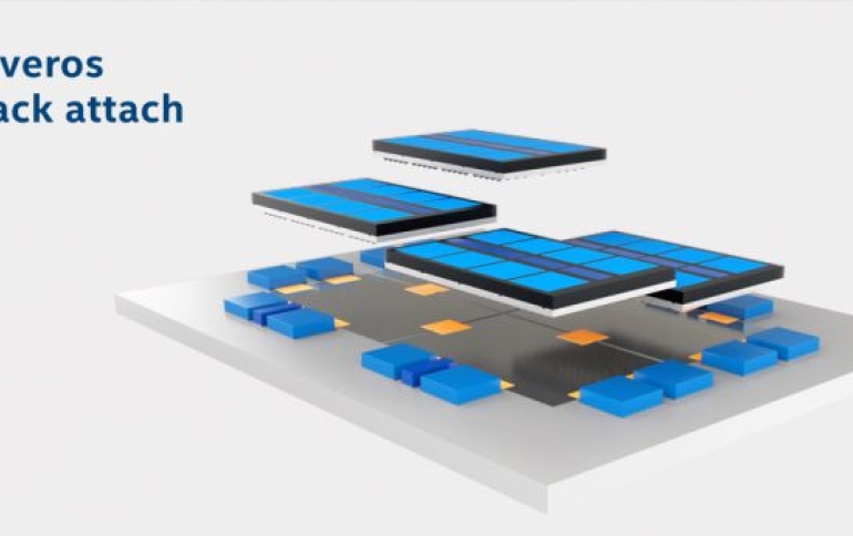
- Co-EMIB: Intel’s EMIB and Foveros technologies leverage high-density interconnects to enable high bandwidth at low power, with I/O density on par with or better than competitive approaches. The company’s new Co-EMIB technology enables the linkage of even more computing performance and capability together. Co-EMIB allows for the interconnection of two or more Foveros elements with essentially the performance of a single chip. And designers can also connect analog, memory and other tiles with very high bandwidth and at very low power. Co-EMIB will likely will see its first use as a way to link CPU and GPU cores in the Aurora supercomputer Intel and Cray won a $500 million contract to deliver before the end of 2021.
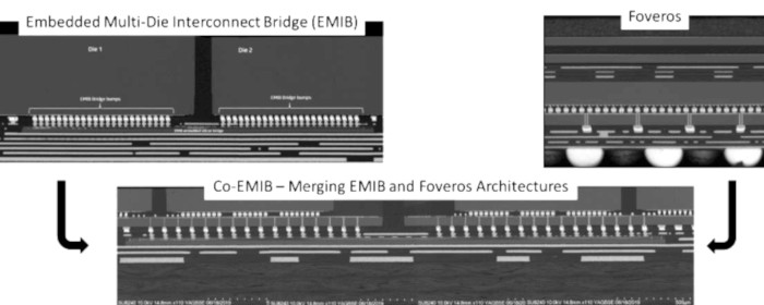
Prototypes shown of Co-EMIB wafers and devices stacked 18 small die on one large one using the Foveros 3D technique Intel announced in December. Two of the devices were then connected using four of its Embedded Multi-die Interconnect Bridge (EMIB) links using 45- and 55-mm bump pitches.
Intel has shipped as many as a million devices using EMIB in Stratix X FPGAs and Kaby Lake G, an integrated CPU/GPU module. Next year it will ship Lakefield, an integrated notebook processor slated to be its first chip using Foveros.
- ODI: Intel’s new Omni-Directional Interconnect provides greater flexibility for communication among chiplets in a package. The top chip can communicate horizontally with other chiplets, similar to EMIB. It can also communicate vertically with through-silicon vias (TSVs) in the base die below, similar to Foveros. And ODI leverages large vertical vias to allow power delivery to the top die directly from the package substrate. Much larger than traditional TSVs, the large vias have lower resistance, providing more robust power delivery simultaneously with higher bandwidth and lower latency enabled through stacking. At the same time, this approach reduces the number of TSVs required in the base die, freeing up more area for active transistors and optimizing die size.
- MDIO: Building upon its Advanced Interface Bus (AIB) PHY level interconnect, Intel disclosed a new die-to-die interface called MDIO. The technology enables a modular approach to system design with a library of chiplet intellectual property blocks. MDIO provides better power efficiency and more than double the pin speed and bandwidth density offered by AIB.Intel claims MDIO is on par with advances rival TSMC announced last month. It will use the interface in chip stacks starting sometime in 2020 but has not decided if it will make the spec open.
Babak Sabi, Intel corporate vice president, Assembly and Test Technology Development said:
“Our vision is to develop leadership technology to connect chips and chiplets in a package to match the functionality of a monolithic system-on-chip. A heterogeneous approach gives our chip architects unprecedented flexibility to mix and match IP blocks and process technologies with various memory and I/O elements in new device form factors. Intel’s vertically integrated structure provides an advantage in the era of heterogeneous integration, giving us an unmatched ability to co-optimize architecture, process and packaging to deliver leadership products”
Chip stacks are widely seen as one of the most significant routes to delivering larger, faster devices. Intel rival TSMC has been using various forms of them for years for everything from smartphone SoCs to high-end FPGAs, GPUs and communications ASICs.
Defining “an Ethernet for chiplets” is the most important goal of DARPA’s CHIPS project, its program manager said last year. Separately, the Open Compute Project launched an effort recently to define open standards for chiplets, but they are still in an early stage.
The new techniques will help shrink packaging interconnects down from 50mm today and drive up their density to tens of thousands of I/Os per mm2 from a couple hundred today, he said.
However, there are several hurdles ahead. “Somewhere between 20-35 microns we will need to transition from solder to non-solder-based interconnects,” said Ravi Mahajan, an Intel fellow.
Yields are as low as 20% on some chip stacks, an even larger challenge. Intel designed a new module for its homegrown chip tester that better determines how individual die perform in a module, pushing yields above 70% for an eight-chip stack.


Very, very interesting news. Where are the chips? :)