Intel Uses Cobalt Interconnect for 10nm, Global Foundries Detail EUV Lithography for 7nm
The IEEE International Electron Device Meeting (IEDM) event kicked off this week in San Fransisco with Intel researchers to describe how they used cobalt for some interconnect layers at 10nm, and GlobalFoudries to talk about extreme ultraviolet (EUV) at the 7nm node.
Intel researchers presented a 10nm logic technology platform claiming that it offers an "excellent transistor and interconnect performance and aggressive design-rule scaling."
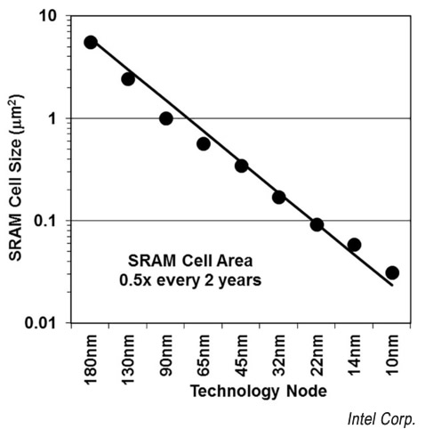
They demonstrated the platform by building a 204Mb SRAM having three different types of memory cells: a high-density 0.0312µm2 cell, a low voltage 0.0367µm2 cell, and a high-performance 0.0441µm2 cell. The platform features 3rd-generation FinFETs fabricated with self-aligned quadruple patterning (SAQP) for critical layers, leading to a 7nm fin width at a 34nm pitch, and a 46nm fin height; a 5th-generation high-k metal gate; and 7th-generation strained silicon.
But what's intrestign is the fact that Intel used cobalt in on the bottom two layers of its 10nm interconnect to get a 5-10x improvement in electromigration and a 2x reduction in via resistance.
NMOS and PMOS current is 71% and 35% greater, respectively, compared to 14nm FinFET transistors. Inte lsaid that metal stacks with four or six workfunctions enable operation at different threshold voltages, and self-aligned gate contacts over active gates are employed.
The graph on the below shows that the new platform maintains traditional scaling trends, while the following photomicrograph the platform's 12-layer interconnect stack.


It is the first time that a chip maker has detailed plans to introduce cobalt - a metal considered a promising dielectric candidate - in a process.
Globalfoundries at 7nm continues to use the copper/low-k dielectrics that have been used by the semiconductor industry for the past several nodes. The company claims that copper/low-k provides reliability benefits, reducing complexity and yield risk.
At the same event, Globalfoundries researchers presented a fully integrated 7nm CMOS platform that provides significant density scaling and performance improvements over 14nm. It features a 3rd-generation FinFET architecture with self-aligned quadruple patterning (SAQP) used for fin formation, and self-aligned double patterning for metallization (SADP).
However, the company said that the technology platform was also designed to leverage EUV insertion for specific multi-patterned (MP) levels in order to improve cycle time and manufacturing efficiency.
Globalfoundries said that specific parameters in EUV still need to be worked out, referring to pellicle and inspection technologies. However, the company is currently installing its first EUV production tools at its Fab 8 in upstate New York.
Globalfoundries said that the 7nm platform features an improvement of 2.8x in routed logic density, along with impressive performance/power responses versus 14nm: a >40% performance increase at a fixed power, or alternatively a power reduction of >55% at a fixed frequency.
The researchers demonstrated the platform by using it to build an incredibly small 0.0269µm2 SRAM cell. Multiple Cu/low-k BEOL stacks are possible for a range of system-on-chip (SoC) applications, and a multi-workfunction process makes possible a range of threshold voltages for diverse applications.
Globalfoundries offers a complete set of foundation and complex IP (intellectual property) in this advanced CMOS platform for both high-performance computing and mobile applications.
Although both Intel and GFO presentations lacked in-depth technical details, the improvements in logic transistor density compared to previous generation of processes is almost on pace with Moore's Law.


