Key Samsung Technologies That Enabled 10nm-Class DRAM
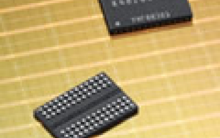
Samsung Electronics in April became the first manufacturer to mass produce 10nm-class 8Gb (gigabit) DDR4 DRAM, taking the lead in advancing DRAM technology. Let’s take a closer look at the core technological breakthroughs that led to the successful mass production of 10nm-class DRAM.
A single DRAM chip contains anywhere from hundreds of millions of cells to billions of them, depending on data capacity. Each cell consists of two parts: a capacitor that stores data in the form of an electrical charge, and a transistor that controls access to it. The two parts are collectively referred to as a DRAM cell. The latest DRAM from Samsung is an 8Gb (gigabit) chip, meaning it has more than 8 billion cells.
The DRAM chip is produced from a very thin silicon board called a "wafer." As the circuit design and process technology-which are applied to a wafer-become more refined, the wafer is able to produce more chips.
A single 10nm-class DRAM wafer developed by Samsung produces more than 1,000 chips, which is 30 percent more than what could be produced on a 20nm DRAM wafer.
Using the new 10nm-class manufacturing technology, 30 percent more chips can be produced from a single wafer than from a 20nm wafer.
Samsung developed three innovative technologies to successfully mass produce 10nm-class DRAM: Samsung’s proprietary cell design technology, QPT (quadruple patterning technology), and ultra-thin dielectric layer deposition.
In semiconductor engineering, the core of the business is designing and integrating nanometer-scale circuits onto a small, nail-sized chip. The photolithography process refers to printing electric circuit patterns on a wafer in a way that resembles printing a photo. While a basic photolithography process prints a single pattern, multiple patterning technologies, like double patterning technology (DPT) and QPT, print up to two and four patterns respectively. Multiple patterning is widely used for advanced memory products that require a high level of scaling and density.
In case of the QPT used for Samsung’s 10nm-class DRAM, the photolithography process itself is done once and, after that, many steps are added to realize the QPT, as can be seen in the diagram. As a result of these steps, four patterns can be produced in the same surface area. The whole point of multiple patterning is about drawing more circuit patterns in the same space using currently available photolithography technology, thereby maximizing the wafer productivity.

Printing more patterns in the same given space is not the end of the story. A DRAM chip does not function properly if even a single cell-out of hundreds of billions-does not function properly. Therefore, ensuring that all cells work well in a sufficient amount of time is a prerequisite to produce a DRAM chip with high performance and power efficiency. To this end, each and every capacitor (where the electric charges representing data are contained) needs to be thin, long, and sturdy. This is where ultra-fine dielectric layer deposition technology comes in.
Capacitors are used to contain electrical charges (data) temporarily. They can be either charged or discharged to represent the two values of a bit: 1 and 0. When a capacitor contains a sufficient amount of electrons, it can quickly determine the digital signals. Since the manufacturing process only gets more refined, capacitors have to be thinner and longer in order to contain enough electrons.
When constructing a capacitor, it must be covered with a thin but solid dielectric material in order to prevent its electrical charge from leaking and the electrical charges in the surrounding capacitors from causing interference (the space between each capacitor is only a few tens of nanometers). The ability to maintain the uniformity of these dielectric layers is the core technology that determines the quality of the manufacturing and product competitiveness.
With the previous technology for 20nm chips, the dielectric layers were thicker at the top than the bottom, making the capacitors look like upside-down cones. This was not much of a problem. However, as the capacitors and the space between them has become thinner, the dielectric layers have also had to get thinner. To address the problem, Samsung developed a new material through the ultra-fine dielectric deposition technology, successfully making the thickness of the dielectric layers uniform to a few angstroms (tenths of a nanometer). This technical breakthrough allowed the birth of the 10nm-class DRAM with high performance and reliability.
In general, semiconductors consume more power in proportion to the speed at which they operate. Which is why the increase of speed and reduction of power consumption in the new 10nm-class DRAM is so remarkable.
In an idle state, DRAM consumes less energy than when it is operating in an active state. The 10nm-class DRAM is designed to accelerate its performance in controlling and processing data while in an active state and then go back to an idle state as soon as possible. As a result, the 10nm-class DRAM is both faster and more power efficient when processing data.
More specifically, the 10nm-class DRAM operates at 3.2Gbps on PC and server systems (up from the 2.4Gbps of its predecessor), while reducing power consumption by 10 to 20 percent.
Faster speeds can simply be achieved by consuming more power, but energy efficiency is also a very important factor in any computing system, including PC, mobile and server applications. Because of this, achieving higher performance and reducing power consumption at the same time is essential for DRAM products, which are used in all kinds of advanced computing systems today.
Based on its advancements with the new 10nm-class DRAM technology, Samsung expects to also introduce a 10nm-class mobile DRAM solution this year, which is faster and uses less power than currently available mobile DRAM solutions. The new mobile DRAM solution will be able to support battery-dependent mobile devices with high resolution features such as FHD video (which is currently the most common standard) and 4K UHD videos.
Samsung says that productivity and speed of 10nm-class DRAM has increased by more than 30 percent compared to 20nm DRAM, while the power consumption has reduced by 10 to 20 percent.


