NVIDIA Unveils Next Generation CUDA GPU Architecture - Codenamed "Fermi"
Nvidia today officially introduced its next generation CUDA GPU architecture, codenamed "Fermi". An entirely new ground-up design, the "Fermi" architecture is the foundation for the world's first computational graphics processing units (GPUs), promising to deliver breakthroughs in both graphics and GPU computing.
"NVIDIA and the Fermi team have taken a giant step towards making GPUs attractive for a broader class of programs," said Dave Patterson, director Parallel Computing Research Laboratory, U.C. Berkeley and co-author of Computer Architecture: A Quantitative Approach. "I believe history will record Fermi as a significant milestone."
Presented at the company's inaugural GPU Technology Conference, in San Jose, California, "Fermi" delivers a feature set that accelerates performance on a wider array of computational applications than ever before. Joining NVIDIA's press conference was Oak Ridge National Laboratory who announced plans for a new supercomputer that will use NVIDIA GPUs based on the "Fermi" architecture. "Fermi" also garnered the support of leading organizations including Bloomberg, Cray, Dell, HP, IBM and Microsoft.
"It is completely clear that GPUs are now general purpose parallel computing processors with amazing graphics, and not just graphics chips anymore," said Jen-Hsun Huang, co-founder and CEO of NVIDIA. "The Fermi architecture, the integrated tools, libraries and engines are the direct results of the insights we have gained from working with thousands of CUDA developers around the world. We will look back in the coming years and see that Fermi started the new GPU industry."
As the foundation for NVIDIA's family of next generation GPUs namely GeForce, Quadro and Tesla − "Fermi" features a host of new technologies including:
- C++, complementing existing support for C, Fortran, Java, Python, OpenCL and DirectCompute.
- ECC, a critical requirement for datacenters and supercomputing centers deploying GPUs on a large scale
- 512 CUDA Cores featuring the new IEEE 754-2008 floating-point standard, surpassing even the most advanced CPUs
- 8x the peak double precision arithmetic performance over NVIDIA?s last generation GPU. Double precision is critical for high-performance computing (HPC) applications such as linear algebra, numerical simulation, and quantum chemistry
- NVIDIA Parallel DataCache - a cache hierarchy in a GPU that speeds up algorithms such as physics solvers, raytracing, and sparse matrix multiplication where data addresses are not known beforehand
- NVIDIA GigaThread Engine with support for concurrent kernel execution, where different kernels of the same application context can execute on the GPU at the same time (eg: PhysX fluid and rigid body solvers)
- Nexus - a fully integrated heterogeneous computing application development environment within Microsoft Visual Studio
Nvidia described the "Fermi" architecture as the most significant leap forward in GPU architecture since the original G80. G80 was Nvidia's initial vision of what a unified graphics and computing parallel processor should look like. GT200 extended the performance and functionality of G80. With Fermi, Nvidia has taken all they have learned from the two prior processors and all the applications that were written for them, and employed a completely new approach to design to create the world?s first computational GPU.

The key architectural highlights of Fermi are:
Third Generation Streaming Multiprocessor (SM)
o 32 CUDA cores per SM, 4x over GT200
o 8x the peak double precision floating point performance over GT200
o Dual Warp Scheduler that schedules and dispatches two warps of 32 threads per clock
o 64 KB of RAM with a configurable partitioning of shared memory and L1 cache
Second Generation Parallel Thread Execution ISA
o Unified Address Space with Full C++ Support
o Optimized for OpenCL and DirectCompute
o Full IEEE 754-2008 32-bit and 64-bit precision
o Full 32-bit integer path with 64-bit extensions
o Memory access instructions to support transition to 64-bit addressing
o Improved Performance through Predication
Improved Memory Subsystem
o NVIDIA Parallel DataCache hierarchy with Configurable L1 and Unified L2 Caches
o First GPU with ECC memory support
o Greatly improved atomic memory operation performance
NVIDIA GigaThread Engine
o 10x faster application context switching
o Concurrent kernel execution
o Out of Order thread block execution
o Dual overlapped memory transfer engines
 The first Fermi based GPU, implemented with 3.0 billion transistors, features up to 512 CUDA
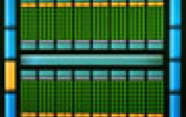
cores. A CUDA core executes a floating point or integer instruction per clock for a thread. The 512 CUDA cores are organized in 16 SMs of 32 cores each. The GPU has six 64-bit memory partitions, for a 384-bit memory interface, supporting up to a total of 6 GB of GDDR5 DRAM memory. A host interface connects the GPU to the CPU via PCI-Express. The GigaThread global scheduler distributes thread blocks to SM thread schedulers.
The third generation SM introduces several architectural innovations that make it not only the most powerful SM yet built, but also the most programmable and efficient, according to Nvidia.
Each SM features 32 CUDA processors' a fourfold increase over prior SM designs. Each CUDA processor has a fully pipelined integer arithmetic logic unit (ALU) and floating point unit (FPU). Prior GPUs used IEEE 754-1985 floating point arithmetic. The Fermi architecture implements the new IEEE 754-2008 floating-point standard, providing the fused multiply-add (FMA) instruction for both single and double precision arithmetic. FMA improves over a multiply-add (MAD) instruction by doing the multiplication and addition with a single final rounding step, with no loss of precision in the addition. FMA is more accurate than performing the operations separately.
GT200 implemented double precision FMA. In GT200, the integer ALU was limited to 24-bit precision for multiply operations; as a result, multi-instruction emulation sequences were required for integer arithmetic. In Fermi, the newly designed integer ALU supports full 32-bit precision for all instructions, consistent with standard programming language requirements. The ALU is optimized to efficiently support 64-bit and extended precision operations. Various instructions are supported, including Boolean, shift, move, compare, convert, bit-field extract, bit-reverse insert, and population count.
Each SM has 16 load/store units, allowing source and destination addresses to be calculated for sixteen threads per clock. Supporting units load and store the data at each address to cache or DRAM.
Double precision arithmetic is at the heart of HPC applications such as linear algebra, numerical simulation, and quantum chemistry. The Fermi architecture has been specifically designed to offer unprecedented performance in double precision; up to 16 double precision fused multiply-add operations can be performed per SM, per clock, a dramatic improvement over the GT200 architecture.

One of the key architectural innovations that greatly improved both the programmability and performance of GPU applications is on-chip shared memory. Shared memory enables threads within the same thread block to cooperate, facilitates extensive reuse of on-chip data, and greatly reduces off-chip traffic. Shared memory is a key enabler for many high-performance CUDA applications. G80 and GT200 have 16 KB of shared memory per SM. In the Fermi architecture, each SM has 64 KB of on-chip memory that can be configured as 48 KB of Shared memory with 16 KB of L1 cache or as 16 KB of Shared memory with 48 KB of L1 cache. For existing applications that make extensive use of Shared memory, tripling the amount of Shared memory yields significant performance improvements, especially for problems that are bandwidth constrained. For existing applications that use Shared memory as software managed cache, code can be streamlined to take advantage of the hardware caching system, while still having access to at least 16 KB of shared memory for explicit thread cooperation.
Best of all, applications that do not use Shared memory automatically benefit from the L1 cache, allowing high performance CUDA programs to be built with minimum time and effort.

Presented at the company's inaugural GPU Technology Conference, in San Jose, California, "Fermi" delivers a feature set that accelerates performance on a wider array of computational applications than ever before. Joining NVIDIA's press conference was Oak Ridge National Laboratory who announced plans for a new supercomputer that will use NVIDIA GPUs based on the "Fermi" architecture. "Fermi" also garnered the support of leading organizations including Bloomberg, Cray, Dell, HP, IBM and Microsoft.
"It is completely clear that GPUs are now general purpose parallel computing processors with amazing graphics, and not just graphics chips anymore," said Jen-Hsun Huang, co-founder and CEO of NVIDIA. "The Fermi architecture, the integrated tools, libraries and engines are the direct results of the insights we have gained from working with thousands of CUDA developers around the world. We will look back in the coming years and see that Fermi started the new GPU industry."
As the foundation for NVIDIA's family of next generation GPUs namely GeForce, Quadro and Tesla − "Fermi" features a host of new technologies including:
- C++, complementing existing support for C, Fortran, Java, Python, OpenCL and DirectCompute.
- ECC, a critical requirement for datacenters and supercomputing centers deploying GPUs on a large scale
- 512 CUDA Cores featuring the new IEEE 754-2008 floating-point standard, surpassing even the most advanced CPUs
- 8x the peak double precision arithmetic performance over NVIDIA?s last generation GPU. Double precision is critical for high-performance computing (HPC) applications such as linear algebra, numerical simulation, and quantum chemistry
- NVIDIA Parallel DataCache - a cache hierarchy in a GPU that speeds up algorithms such as physics solvers, raytracing, and sparse matrix multiplication where data addresses are not known beforehand
- NVIDIA GigaThread Engine with support for concurrent kernel execution, where different kernels of the same application context can execute on the GPU at the same time (eg: PhysX fluid and rigid body solvers)
- Nexus - a fully integrated heterogeneous computing application development environment within Microsoft Visual Studio
Nvidia described the "Fermi" architecture as the most significant leap forward in GPU architecture since the original G80. G80 was Nvidia's initial vision of what a unified graphics and computing parallel processor should look like. GT200 extended the performance and functionality of G80. With Fermi, Nvidia has taken all they have learned from the two prior processors and all the applications that were written for them, and employed a completely new approach to design to create the world?s first computational GPU.

The key architectural highlights of Fermi are:
Third Generation Streaming Multiprocessor (SM)
o 32 CUDA cores per SM, 4x over GT200
o 8x the peak double precision floating point performance over GT200
o Dual Warp Scheduler that schedules and dispatches two warps of 32 threads per clock
o 64 KB of RAM with a configurable partitioning of shared memory and L1 cache
Second Generation Parallel Thread Execution ISA
o Unified Address Space with Full C++ Support
o Optimized for OpenCL and DirectCompute
o Full IEEE 754-2008 32-bit and 64-bit precision
o Full 32-bit integer path with 64-bit extensions
o Memory access instructions to support transition to 64-bit addressing
o Improved Performance through Predication
Improved Memory Subsystem
o NVIDIA Parallel DataCache hierarchy with Configurable L1 and Unified L2 Caches
o First GPU with ECC memory support
o Greatly improved atomic memory operation performance
NVIDIA GigaThread Engine
o 10x faster application context switching
o Concurrent kernel execution
o Out of Order thread block execution
o Dual overlapped memory transfer engines
 The first Fermi based GPU, implemented with 3.0 billion transistors, features up to 512 CUDA
cores. A CUDA core executes a floating point or integer instruction per clock for a thread. The 512 CUDA cores are organized in 16 SMs of 32 cores each. The GPU has six 64-bit memory partitions, for a 384-bit memory interface, supporting up to a total of 6 GB of GDDR5 DRAM memory. A host interface connects the GPU to the CPU via PCI-Express. The GigaThread global scheduler distributes thread blocks to SM thread schedulers.
The third generation SM introduces several architectural innovations that make it not only the most powerful SM yet built, but also the most programmable and efficient, according to Nvidia.
Each SM features 32 CUDA processors' a fourfold increase over prior SM designs. Each CUDA processor has a fully pipelined integer arithmetic logic unit (ALU) and floating point unit (FPU). Prior GPUs used IEEE 754-1985 floating point arithmetic. The Fermi architecture implements the new IEEE 754-2008 floating-point standard, providing the fused multiply-add (FMA) instruction for both single and double precision arithmetic. FMA improves over a multiply-add (MAD) instruction by doing the multiplication and addition with a single final rounding step, with no loss of precision in the addition. FMA is more accurate than performing the operations separately.
GT200 implemented double precision FMA. In GT200, the integer ALU was limited to 24-bit precision for multiply operations; as a result, multi-instruction emulation sequences were required for integer arithmetic. In Fermi, the newly designed integer ALU supports full 32-bit precision for all instructions, consistent with standard programming language requirements. The ALU is optimized to efficiently support 64-bit and extended precision operations. Various instructions are supported, including Boolean, shift, move, compare, convert, bit-field extract, bit-reverse insert, and population count.
Each SM has 16 load/store units, allowing source and destination addresses to be calculated for sixteen threads per clock. Supporting units load and store the data at each address to cache or DRAM.
Double precision arithmetic is at the heart of HPC applications such as linear algebra, numerical simulation, and quantum chemistry. The Fermi architecture has been specifically designed to offer unprecedented performance in double precision; up to 16 double precision fused multiply-add operations can be performed per SM, per clock, a dramatic improvement over the GT200 architecture.

One of the key architectural innovations that greatly improved both the programmability and performance of GPU applications is on-chip shared memory. Shared memory enables threads within the same thread block to cooperate, facilitates extensive reuse of on-chip data, and greatly reduces off-chip traffic. Shared memory is a key enabler for many high-performance CUDA applications. G80 and GT200 have 16 KB of shared memory per SM. In the Fermi architecture, each SM has 64 KB of on-chip memory that can be configured as 48 KB of Shared memory with 16 KB of L1 cache or as 16 KB of Shared memory with 48 KB of L1 cache. For existing applications that make extensive use of Shared memory, tripling the amount of Shared memory yields significant performance improvements, especially for problems that are bandwidth constrained. For existing applications that use Shared memory as software managed cache, code can be streamlined to take advantage of the hardware caching system, while still having access to at least 16 KB of shared memory for explicit thread cooperation.
Best of all, applications that do not use Shared memory automatically benefit from the L1 cache, allowing high performance CUDA programs to be built with minimum time and effort.


