Samsung Announces 32nm 'Saratoga' and Dual CORTEX A9 'Orion' Mobile Processors
Samsung today held the seventh Samsung Mobile Solutions Forum at the Westin Taipei Hotel, where it highlighted mobile device trends, showcasesed new mobile processors, memory solutions and shared insight into future mobile technologies.
Attended industry professionals, the annual event featured a "Smart and Green Mobility Plus" theme that emphasized the increasingly interconnected, foundational role of high performance and low-power benefits in enabling advanced solutions for mobile devices.
New smart mobile technologies highlighted at this year's forum included a 1GHz dual core application processor designed on low-power process technology, an engineering sample of the world's first application processor utilizing 32 nanometer (nm) low-power process technology with high-k metal gate technology, advanced image sensor ICs featuring low light sensitivity with backside illumination and a high-performance 16gigabyte moviNAND chip with an eMMC4.41 interface.
First Mobile Application Processor in 32nm High-K Metal Gate Low Power Logic Process
Samsung highlighted an engineering sample of its application processor using its 32 nanometer (nm) low power High-K Metal Gate (HKMG) logic process.
Codenamed Saratoga, this new application processor was designed to provide a low power, high performance, and cost effective solution for next generation consumer electronic (CE) products such as personal navigation devices (PND), electronics dictionaries, and e-book readers.
"We announced, in June this year, the successful qualification of our 32nm HKMG low power logic process and design ecosystem," said Dr. Kwang-hyun Kim, senior vice president of System LSI Sales and Marketing, Samsung Electronics. "Saratoga is the world's first application processor that is implemented in this 32nm process which offers lower leakage current, higher performance, and higher gate density. We are excited to demonstrate such capability through this chip."
Likes its 45nm predecessor, S5P6440, the 32nm Saratoga application processor is based on an ARM1176 CPU core. It features 2D graphics acceleration hardware that supports the OpenVG application programming interface (API) standard.
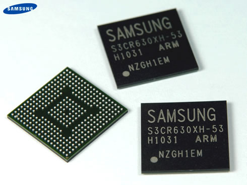
In addition to integrating peripherals and memory interface commonly used in many CE products to reduce BOM cost, Saratoga is also equipped with a mobile industry processor interface (MIPI) display serial interface (DSI) which minimizes the EMI and lowers the number of pins needed to connect with the display panel, greatly reducing design complexity and cost.
Dual CORTEX - A9 Application Processor for Mobile Devices
Samsung also today introduced its new 1GHz ARM CORTEX A9-based dual-core application processor, codenamed Orion, for mobile applications.
The powerful dual processor chip platform has been designed specifically to meet the needs of high-performance, low-power mobile applications including tablets, netbooks and smartphones.
"Consumers are demanding the full web experience without compromise while on the go," said Dojun Rhee, vice president of Marketing, System LSI Division, Samsung Electronics. "Given this trend, mobile device designers need an application processor platform that delivers superb multimedia performance, fast CPU processing speed, and abundant memory bandwidth. Samsung's newest dual core application processor chip is designed specifically to fulfill such stringent performance requirements while maintaining long battery life."

Designed using Samsung's 45 nanometer low-power process technology, Orion features a pair of 1GHz ARM Cortex A9 cores, each comes with a 32KB data cache and a 32KB instruction cache. Samsung also included a 1MB L2 cache to optimize CPU processing performance and provide fast context switching in a multi-tasking environment. In addition, the memory interface and bus architecture of Orion supports data intensive multimedia applications including full HD video playback and high speed 3D action games.
Samsung's new application processor supports advanced multimedia features implemented by hardware accelerators, such as video encoder/decoder that supports 30fps video playback and recording at 1080P full HD resolution. Using an enhanced graphics processing unit (GPU), the new processors are capable of delivering 5 times the 3D graphics performance over the previous processor generation from Samsung.
For design flexibility and system BOM cost reduction, Orion integrates a set of interfaces commonly used in mobile devices to configure various peripheral functionalities. For example, with this processor, Samsung's customers have the choice to use different types of storage including NAND flash, moviNAND, SSD or HDD providing both SATA, and eMMC interfaces. Customers can also choose their appropriate memory options including low power LPDDR2 or DDR3, which is commonly used for high performance. In addition, a global positioning system (GPS) receiver baseband processor is embedded in the processor to seamlessly support location based services (LBS), which is critical in many emerging mobile applications.
Orion features an onboard native triple display controller architecture that compliments multi-tasking operations in a multiple display environment. A mobile device using the Orion processor can simultaneously support two on-device display screens, while driving a third external display such as a TV or a monitor, via an on-chip HDMI 1.3a interface.
Orion is designed to support package-on-package (POP) with memory stacking to reduce the footprint. A derivative of Orion, which is housed in a standalone package with a 0.8mm ball pitch, is also available.
Samsung's new dual-core application processor, Orion, will be available to Samsung's select customers in the fourth quarter of 2010 and is scheduled for mass production in the first half of 2011.
Embedded NAND Flash for Smartphones
At the same event, Samsung introduced high-performance 8-gigabyte (GB) and 16GB moviNAND embedded memory chips for use in smartphones.
The new solutions are the first memory devices in the industry fully compatible with the latest e-MMC specification, the JEDEC's Embedded MultiMediaCard Product Standard v4.41.
Adopting the new higher performance e-MMC 4.41 specification, Samsung's moviNAND can operate more efficiently than previous solutions developed under the e-MMC 4.4 specification by providing features that improve the responsiveness of the e-MMC device to the host (or application processor).
"We have already been providing new moviNAND solutions compatible with e-MMC v4.41 to a few key customers and getting a very positive response from them," said Seijin Kim, vice president, Flash Memory Planning/Enabling, Samsung Electronics. "These solutions are consistent with our commitment to provide a diversity of technologies for embedded memory to enhance its user-friendliness, in contributing to the rapid growth of the smartphone market."
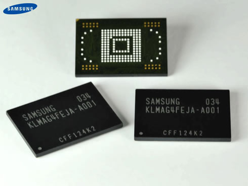
Previously the e-MMC 4.4 interface has offered designers the flexibility of partitioning storage, such as using the single-level cell (SLC) area for high speed operations and the multi-level cell (MLC) area for high density data storage. Now, the new chips (adhering to the new e-MMC 4.41 interface standard) provide a significantly upgraded user experience, with a high priority interrupt (HPI) and improved background operation features.
Embracing the new standardized features, the latest Samsung moviNAND chips enable more efficient processing of orders. If the host wants to execute an application or read data while the e-MMC device is writing data, the host can send an HPI command to the device so that the device stops previous writing to respond to the newest command. Using this feature, the host can receive the device's response without any latency.
Also, when the Samsung embedded memory is not in operation, the host can command it to utilize the free time for background operations such as garbage compaction, so that the embedded memory can reduce the write latency.
In addition to its new high-performance moviNAND, Samsung is introducing ultra-thin five chip MCP (multi-chip package) solutions which measure just 1 millimeter (mm), a significant reduction over current four-chip MCPs that are 1.15mm in height (z-height). The moviNAND-based MCP will be available in combination with mobile DRAM. The advanced multipurpose MCP offerings will be available by the end of this year for use in mobile applications with high multimedia workload such as smartphones.
Samsung already started producing 8GB moviNAND, using 30 nanometer (nm) class 32-gigabit (Gb) NAND flash chips in late July, and will start producing 16GB moviNAND using 20nm-class 32Gb NAND flash this month.
Samsung plans to start replacing its 30nm-class 32Gb NAND flash chips with a full line of 20nm-class 32Gb NAND chips for future moviNAND products later this year.
New CMOS Imagers
Samsung also announced two new 1.4 micron CMOS imagers, the S5K4E5 and S5K2N1, adopting back side illuminated (BSI) pixel technology.
Each imager is optimized for target applications such as smartphones for the S5K4E5 and digital still cameras (DSC) and digital video cameras (DVC) for the S5K2N1.
"The demand for higher quality images and video with ever shrinking pixel size has pushed the new technology innovation curve in CMOS imagers," said Dojun Rhee, vice president of Marketing, System LSI Division, Samsung Electronics. "As such, CMOS image technology has become even more competitive in digital camera and video products that have been traditionally dominated by CCD technology. A small pixel size combined with best-in-class sensitivity under low light for still and video capture makes Samsung's newest imagers ideal for traditional handheld cameras as well as smartphones."
In contrast to the front side illumination technology, backside illumination collects photons from the backside of the pixel. The reversed structure moves the photodiode to the top maximizing photoelectric efficiency as the light is not scattered through the metal wiring and dielectric layers, which cause the loss of photons. Adoption of the BSI technology addresses the low light sensitivity concern common to CMOS image sensors as the pixel size reduces.

Samsung's new BSI imagers show 30 percent enhancement in low light sensitivity over conventional front side illumination imagers of the same pixel size. By optimizing process parameters, Samsung was able to efficiently control crosstalk thereby improving the color, electrical and optical performance significantly.
The S5K4E5, a quarter-inch optical format 1.4 micron 5 megapixel (Mp) CMOS image sensor, is designed to support full resolution real-time video. By providing 30 frames per second (fps) full resolution frame rates it also enables the user to 'catch the shot' by capturing the frame as the user hits the shutter button thus reducing shot to shot lag time. The 5Mp imager has a wider chief ray angle that reduces the height of the imager package making it attractive for slim, small form factor smartphones with demanding z-height requirements.
The S5K2N1, a 1/2.33 inch optical format 1.4 micron 14.6Mp imager, offers 30fps capability at full resolution and leverages Samsung's low-power 90 nanometer logic process technology. Samsung is able to offer a dedicated thermal enhanced plastic lead ceramic carrier (TePLCC) package to more effectively dissipate the heat generated by the high performance device.
These imagers also offer the ability to capture full high definition (HD) resolution video images at 60fps.
Samples of the 5Mp S5K4E5 are available now with mass production starting in the fourth quarter of this year. The 14.6Mp S5K2N1 is expected to start sampling in the fourth quarter of 2010 with production scheduled in the first quarter of 2011.
New smart mobile technologies highlighted at this year's forum included a 1GHz dual core application processor designed on low-power process technology, an engineering sample of the world's first application processor utilizing 32 nanometer (nm) low-power process technology with high-k metal gate technology, advanced image sensor ICs featuring low light sensitivity with backside illumination and a high-performance 16gigabyte moviNAND chip with an eMMC4.41 interface.
First Mobile Application Processor in 32nm High-K Metal Gate Low Power Logic Process
Samsung highlighted an engineering sample of its application processor using its 32 nanometer (nm) low power High-K Metal Gate (HKMG) logic process.
Codenamed Saratoga, this new application processor was designed to provide a low power, high performance, and cost effective solution for next generation consumer electronic (CE) products such as personal navigation devices (PND), electronics dictionaries, and e-book readers.
"We announced, in June this year, the successful qualification of our 32nm HKMG low power logic process and design ecosystem," said Dr. Kwang-hyun Kim, senior vice president of System LSI Sales and Marketing, Samsung Electronics. "Saratoga is the world's first application processor that is implemented in this 32nm process which offers lower leakage current, higher performance, and higher gate density. We are excited to demonstrate such capability through this chip."
Likes its 45nm predecessor, S5P6440, the 32nm Saratoga application processor is based on an ARM1176 CPU core. It features 2D graphics acceleration hardware that supports the OpenVG application programming interface (API) standard.

In addition to integrating peripherals and memory interface commonly used in many CE products to reduce BOM cost, Saratoga is also equipped with a mobile industry processor interface (MIPI) display serial interface (DSI) which minimizes the EMI and lowers the number of pins needed to connect with the display panel, greatly reducing design complexity and cost.
Dual CORTEX - A9 Application Processor for Mobile Devices
Samsung also today introduced its new 1GHz ARM CORTEX A9-based dual-core application processor, codenamed Orion, for mobile applications.
The powerful dual processor chip platform has been designed specifically to meet the needs of high-performance, low-power mobile applications including tablets, netbooks and smartphones.
"Consumers are demanding the full web experience without compromise while on the go," said Dojun Rhee, vice president of Marketing, System LSI Division, Samsung Electronics. "Given this trend, mobile device designers need an application processor platform that delivers superb multimedia performance, fast CPU processing speed, and abundant memory bandwidth. Samsung's newest dual core application processor chip is designed specifically to fulfill such stringent performance requirements while maintaining long battery life."

Designed using Samsung's 45 nanometer low-power process technology, Orion features a pair of 1GHz ARM Cortex A9 cores, each comes with a 32KB data cache and a 32KB instruction cache. Samsung also included a 1MB L2 cache to optimize CPU processing performance and provide fast context switching in a multi-tasking environment. In addition, the memory interface and bus architecture of Orion supports data intensive multimedia applications including full HD video playback and high speed 3D action games.
Samsung's new application processor supports advanced multimedia features implemented by hardware accelerators, such as video encoder/decoder that supports 30fps video playback and recording at 1080P full HD resolution. Using an enhanced graphics processing unit (GPU), the new processors are capable of delivering 5 times the 3D graphics performance over the previous processor generation from Samsung.
For design flexibility and system BOM cost reduction, Orion integrates a set of interfaces commonly used in mobile devices to configure various peripheral functionalities. For example, with this processor, Samsung's customers have the choice to use different types of storage including NAND flash, moviNAND, SSD or HDD providing both SATA, and eMMC interfaces. Customers can also choose their appropriate memory options including low power LPDDR2 or DDR3, which is commonly used for high performance. In addition, a global positioning system (GPS) receiver baseband processor is embedded in the processor to seamlessly support location based services (LBS), which is critical in many emerging mobile applications.
Orion features an onboard native triple display controller architecture that compliments multi-tasking operations in a multiple display environment. A mobile device using the Orion processor can simultaneously support two on-device display screens, while driving a third external display such as a TV or a monitor, via an on-chip HDMI 1.3a interface.
Orion is designed to support package-on-package (POP) with memory stacking to reduce the footprint. A derivative of Orion, which is housed in a standalone package with a 0.8mm ball pitch, is also available.
Samsung's new dual-core application processor, Orion, will be available to Samsung's select customers in the fourth quarter of 2010 and is scheduled for mass production in the first half of 2011.
Embedded NAND Flash for Smartphones
At the same event, Samsung introduced high-performance 8-gigabyte (GB) and 16GB moviNAND embedded memory chips for use in smartphones.
The new solutions are the first memory devices in the industry fully compatible with the latest e-MMC specification, the JEDEC's Embedded MultiMediaCard Product Standard v4.41.
Adopting the new higher performance e-MMC 4.41 specification, Samsung's moviNAND can operate more efficiently than previous solutions developed under the e-MMC 4.4 specification by providing features that improve the responsiveness of the e-MMC device to the host (or application processor).
"We have already been providing new moviNAND solutions compatible with e-MMC v4.41 to a few key customers and getting a very positive response from them," said Seijin Kim, vice president, Flash Memory Planning/Enabling, Samsung Electronics. "These solutions are consistent with our commitment to provide a diversity of technologies for embedded memory to enhance its user-friendliness, in contributing to the rapid growth of the smartphone market."

Previously the e-MMC 4.4 interface has offered designers the flexibility of partitioning storage, such as using the single-level cell (SLC) area for high speed operations and the multi-level cell (MLC) area for high density data storage. Now, the new chips (adhering to the new e-MMC 4.41 interface standard) provide a significantly upgraded user experience, with a high priority interrupt (HPI) and improved background operation features.
Embracing the new standardized features, the latest Samsung moviNAND chips enable more efficient processing of orders. If the host wants to execute an application or read data while the e-MMC device is writing data, the host can send an HPI command to the device so that the device stops previous writing to respond to the newest command. Using this feature, the host can receive the device's response without any latency.
Also, when the Samsung embedded memory is not in operation, the host can command it to utilize the free time for background operations such as garbage compaction, so that the embedded memory can reduce the write latency.
In addition to its new high-performance moviNAND, Samsung is introducing ultra-thin five chip MCP (multi-chip package) solutions which measure just 1 millimeter (mm), a significant reduction over current four-chip MCPs that are 1.15mm in height (z-height). The moviNAND-based MCP will be available in combination with mobile DRAM. The advanced multipurpose MCP offerings will be available by the end of this year for use in mobile applications with high multimedia workload such as smartphones.
Samsung already started producing 8GB moviNAND, using 30 nanometer (nm) class 32-gigabit (Gb) NAND flash chips in late July, and will start producing 16GB moviNAND using 20nm-class 32Gb NAND flash this month.
Samsung plans to start replacing its 30nm-class 32Gb NAND flash chips with a full line of 20nm-class 32Gb NAND chips for future moviNAND products later this year.
New CMOS Imagers
Samsung also announced two new 1.4 micron CMOS imagers, the S5K4E5 and S5K2N1, adopting back side illuminated (BSI) pixel technology.
Each imager is optimized for target applications such as smartphones for the S5K4E5 and digital still cameras (DSC) and digital video cameras (DVC) for the S5K2N1.
"The demand for higher quality images and video with ever shrinking pixel size has pushed the new technology innovation curve in CMOS imagers," said Dojun Rhee, vice president of Marketing, System LSI Division, Samsung Electronics. "As such, CMOS image technology has become even more competitive in digital camera and video products that have been traditionally dominated by CCD technology. A small pixel size combined with best-in-class sensitivity under low light for still and video capture makes Samsung's newest imagers ideal for traditional handheld cameras as well as smartphones."
In contrast to the front side illumination technology, backside illumination collects photons from the backside of the pixel. The reversed structure moves the photodiode to the top maximizing photoelectric efficiency as the light is not scattered through the metal wiring and dielectric layers, which cause the loss of photons. Adoption of the BSI technology addresses the low light sensitivity concern common to CMOS image sensors as the pixel size reduces.

Samsung's new BSI imagers show 30 percent enhancement in low light sensitivity over conventional front side illumination imagers of the same pixel size. By optimizing process parameters, Samsung was able to efficiently control crosstalk thereby improving the color, electrical and optical performance significantly.
The S5K4E5, a quarter-inch optical format 1.4 micron 5 megapixel (Mp) CMOS image sensor, is designed to support full resolution real-time video. By providing 30 frames per second (fps) full resolution frame rates it also enables the user to 'catch the shot' by capturing the frame as the user hits the shutter button thus reducing shot to shot lag time. The 5Mp imager has a wider chief ray angle that reduces the height of the imager package making it attractive for slim, small form factor smartphones with demanding z-height requirements.
The S5K2N1, a 1/2.33 inch optical format 1.4 micron 14.6Mp imager, offers 30fps capability at full resolution and leverages Samsung's low-power 90 nanometer logic process technology. Samsung is able to offer a dedicated thermal enhanced plastic lead ceramic carrier (TePLCC) package to more effectively dissipate the heat generated by the high performance device.
These imagers also offer the ability to capture full high definition (HD) resolution video images at 60fps.
Samples of the 5Mp S5K4E5 are available now with mass production starting in the fourth quarter of this year. The 14.6Mp S5K2N1 is expected to start sampling in the fourth quarter of 2010 with production scheduled in the first quarter of 2011.


