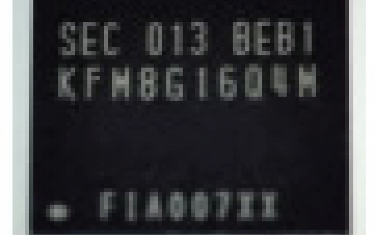
Samsung Announces New 8Gb NAND Memory
Samsung today announced availability of an eight gigabit (Gb) OneNAND chip that takes advantage of advanced 30 nanometer (nm) class process technology.
Based on a single-level-cell (SLC) NAND flash design, the new OneNAND addresses the need for more code data storage in smartphones. The high-density OneNAND memory is now sampling with volume production scheduled by the end of this month.
 The 8Gb OneNAND features the reliability of a SLC design and the performance of OneNAND, which reads data at 70 megabytes per second (MB/s), more than four times the speed of conventional NAND (17MB/s). These characteristics and a low-voltage design make it a particularly attractive solution for handling the growing amount of code data used with touch screens and other high resolution smartphone features. In addition, by applying advanced 30nm-class process technology, Samsung is able to raise productivity by 40 percent over its previous 40nm-class design.
Since 2004, Samsung has expanded the adoption of its OneNAND as a high-performance solution that can be applied to handset applications without having to develop separate software.
OneNAND memory can be used as buffer memory not only for 'writes' in the system ? thanks to its faster-than-NAND 'write' speeds, but also as a buffer for faster, high-performing 'read' operations thank to its NOR flash interface.
According to market research firm, iSuppli, the demand for embedded NAND flash in mobile handsets is expected to reach 1.1 billion units (1 gigabyte (GB) equivalents) in 2010 and more than doubling to 2.5 billion 1GB equivalent units in 2011. Moreover, the Strategic Analysis firm forecasts that demand for smartphones will reach 285 million units in 2010 and grow to 580 million units in 2013.


