Samsung Launches First 3rd-generation (16GB) HBM2E
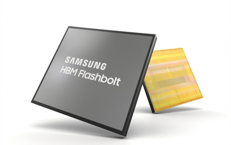
Samsung Electronics today announced the market launch of ‘Flashbolt’, its third-generation High Bandwidth Memory 2E (HBM2E).
The new 16-gigabyte (GB) HBM2E is suited to maximize high performance computing (HPC) systems and help system manufacturers to advance their supercomputers, AI-driven data analytics and graphics systems in a timely manner.
Ready to deliver twice the capacity of the previous-generation 8GB HBM2 ‘Aquabolt’, the new Flashbolt also increases performance and power efficiency. The 16GB capacity is achieved by vertically stacking eight layers of 10nm-class (1y) 16-gigabit (Gb) DRAM dies on top of a buffer chip. This HBM2E package is then interconnected in a precise arrangement of more than 40,000 ‘through silicon via’ (TSV) microbumps, with each 16Gb die containing over 5,600 of these microscopic holes.
Samsung’s Flashbolt provides a data transfer speed of 3.2 gigabits per second (Gbps) by leveraging a proprietary optimized circuit design for signal transmission, while offering a memory bandwidth of 410GB/s per stack. Samsung’s HBM2E can also attain a transfer speed of 4.2Gbps, the maximum tested data rate to date, enabling up to a 538GB/s bandwidth per stack in certain future applications. This would represent a 1.75x enhancement over Aquabolt’s 307GB/s.
Samsung expects to begin volume production during the first half of this year.
Last month, JEDEC published an updated revision of the HBM2 standard. The updated standard added support for even faster memory speeds of up to 3.2Gbps/pin, and in the process pushed the fastest speed for a complete stack of HBM2 memory to 410GB/sec.


