SK hynix Develops Industry’s First 1c DDR5
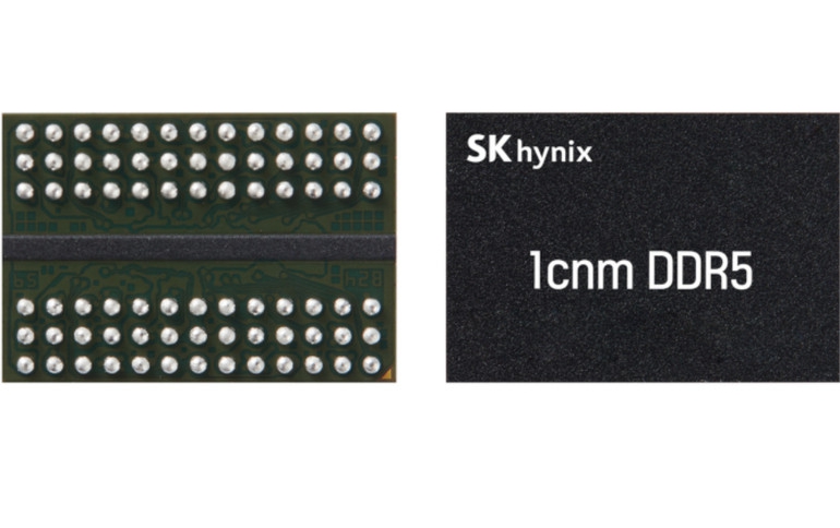
SK hynix Inc. (or “the company”, www.skhynix.com) announced today that it has developed the industry’s first 16Gb DDR5 built using its 1c node, the sixth generation of the 10nm process.
The success marks the beginning of the extreme scaling to the level closer to 10nm in the memory process technology.
The degree of difficulty to advance the shrinking process of the 10nm-range DRAM technology has grown over generations, but SK hynix has become the first in the industry to overcome the technological limitations by raising the level of completion in design, thanks to its industry-leading technology of the 1b, the fifth generation of the 10nm process.
SK hynix said it will be ready for mass production of the 1c DDR5 within the year to start volume shipment next year.
In order to reduce potential errors stemming from the procedure of advancing the process and transfer the advantage of the 1b, which is widely applauded for its best performing DRAM, in the most efficient way, the company extended the platform of the 1b DRAM for development of 1c.
The new product comes with an improvement in cost competitiveness, compared with the previous generation, by adopting a new material in certain process of the extreme ultra violet, or EUV, while optimizing the EUV application process of total. SK hynix also enhanced productivity by more than 30% through technological innovation in design.
The operating speed of the 1c DDR5, expected to be adopted for high-performance data centers, is improved by 11% from the previous generation, to 8Gbps. With power efficiency also improved by more than 9%, SK hynix expects adoption of 1c DRAM to help data centers reduce the electricity cost by as much as 30% at a time when advancement of AI era is leading to an increase in power consumption.
“We are committed to providing differentiated values to customers by applying the 1c technology equipped with the best performance and cost competitiveness to our major next-generation products including HBM1, LPDDR62, and GDDR73,” said Head of DRAM Development Kim Jonghwan. “We will continue to work towards maintaining the leadership in the DRAM space and position as the most-trusted AI memory solution provider.”
1HBM(High Bandwidth Memory): a high-value, high-performance memory that vertically interconnects multiple DRAM chips and dramatically increases data processing speed in comparison to conventional DRAM products. Since the introduction of the first HBM, the generation has shifted to HBM2, HBM2E, HBM3, HBM3E, HBM4 and HBM4E.
2LPDDR: low power DRAM for mobile devices, including smartphones and tablets, which aims to minimize power consumption and features low voltage operation. The latest specifications are for the 7th generation, succeeding the series that end with 1, 2, 3, 4, 4X, 5 and 5X.
3GDDR(Graphics DDR): a standard specification of graphics DRAM defined by the Joint Electron Device Engineering Council (JEDEC) and specialized for processing graphics more quickly. Its generation has shifted from GDDR3, GDDR5, GDDR5X, GDDR6 to GDDR7. With the newer generation promising faster speed and higher power efficiency, GDDR has now become one of the most popular memory chips for AI.


