Sony Develops Blue-violet Semiconductor Laser With An Output Of 100 Watt
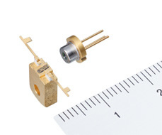
Professor Hiroyuki Yokoyama of the New Industry Creation Hatchery Center (NICHe), Tohoku University and Advanced Materials Laboratories, Sony, have jointly developed a blue-violet semiconductor laser that could be used in large-capacity optical disc storage and for nano-fabrication.
The new laser features a dramatically improved peak laser beam output level, which is almost 100 times higher than the output provided by the currently available lasers.
The 405 nanometer laser is capable of generating optical pulses with a duration of just 3 picoseconds (1 picosecond = one-trillionth of a second), with an ultrahigh output peak power of 100 watts and a repetition frequency of 1 gigahertz.
 To achieve these impressive performance, Tohoku University and Sony have developed a proprietarily GaN-based mode-locked semiconductor laser as well as a new
semiconductor optical amplifier. A mode-locked semiconductor laser is a type of semiconductor laser that emits ultrafast optical pulses. It operates by sending optical pulses with an ultrafast duration in the order of picoseconds (or less) back and forth within the laser cavity. A semiconductor optical amplifier is an optical amplifier that can amplify the laser beam directly using a semiconductor. Although the structure is similar to that of a semiconductor laser, the beam-amplifying functionality is enhanced through antireflective fabrication of the laser facets.
Until now, only solid-state lasers could offer such a high outputs. These lasers use solid crystals such as rubies as the laser medium and they were mainly used for leading-edge chemical research applications. However,the light source box of these laser units was bulky and more further engineering was required to ensure the stable operation of the laser.
Sony claims that the new semiconductor laser system could be applied in a wide range of future applications. For instance, this technology enables the size of components such as the light source box to be drastically reduced.
The high-output, ultrafast pulsed semiconductor laser light source is capable of using a nonlinear optical process known as two-photon absorption (TPA), which occurs only as a result of high intensity optical pulses: When a substance interacts with extremely intense light, the substance does not always respond in proportion to the electromagnetic field of the light, thus creating a prismatic effect. TPA is the phenomenon of absorbing two photons simultaneously to excite the eigenstate corresponding to the resulting sum of photon energy. Using this phenomenon to focus light from an intense laser beam on a lens will result in an extremely high density of power in the vicinity of the focus point.
When light from the laser beam is concentrated on the lens, it creates chemical and thermal changes in the vicinity of the lens focus spot which is narrower than even the diameter of the focus spot of the lens itself. It is anticipated that application of these properties will be possible in a wide range of fields such as three-dimensional (3D) nano-fabrication of inorganic/organic materials in the order of nanometers, and next-generation large-capacity optical disc storage.
Sony tested the principles for applying this technology in next-generation large-capacity optical disc-storage by creating void marks with a diameter of approximately 300 nanometers at intervals of 3 micrometers on the interior of plastic material, and successfully read these marks with the laser beam.
Performance characteristics of an experimental blue-violet ultrafast pulsed semiconductor laser
- Laser wavelength: 405 nm (GaN-based semiconductor laser)
- Peak optical output: 100W or more
- Repetition frequency: 1 GHz
- Pulse width: 3 ps
The 405 nanometer laser is capable of generating optical pulses with a duration of just 3 picoseconds (1 picosecond = one-trillionth of a second), with an ultrahigh output peak power of 100 watts and a repetition frequency of 1 gigahertz.
 To achieve these impressive performance, Tohoku University and Sony have developed a proprietarily GaN-based mode-locked semiconductor laser as well as a new
semiconductor optical amplifier. A mode-locked semiconductor laser is a type of semiconductor laser that emits ultrafast optical pulses. It operates by sending optical pulses with an ultrafast duration in the order of picoseconds (or less) back and forth within the laser cavity. A semiconductor optical amplifier is an optical amplifier that can amplify the laser beam directly using a semiconductor. Although the structure is similar to that of a semiconductor laser, the beam-amplifying functionality is enhanced through antireflective fabrication of the laser facets.
Until now, only solid-state lasers could offer such a high outputs. These lasers use solid crystals such as rubies as the laser medium and they were mainly used for leading-edge chemical research applications. However,the light source box of these laser units was bulky and more further engineering was required to ensure the stable operation of the laser.
Sony claims that the new semiconductor laser system could be applied in a wide range of future applications. For instance, this technology enables the size of components such as the light source box to be drastically reduced.
The high-output, ultrafast pulsed semiconductor laser light source is capable of using a nonlinear optical process known as two-photon absorption (TPA), which occurs only as a result of high intensity optical pulses: When a substance interacts with extremely intense light, the substance does not always respond in proportion to the electromagnetic field of the light, thus creating a prismatic effect. TPA is the phenomenon of absorbing two photons simultaneously to excite the eigenstate corresponding to the resulting sum of photon energy. Using this phenomenon to focus light from an intense laser beam on a lens will result in an extremely high density of power in the vicinity of the focus point.
When light from the laser beam is concentrated on the lens, it creates chemical and thermal changes in the vicinity of the lens focus spot which is narrower than even the diameter of the focus spot of the lens itself. It is anticipated that application of these properties will be possible in a wide range of fields such as three-dimensional (3D) nano-fabrication of inorganic/organic materials in the order of nanometers, and next-generation large-capacity optical disc storage.
Sony tested the principles for applying this technology in next-generation large-capacity optical disc-storage by creating void marks with a diameter of approximately 300 nanometers at intervals of 3 micrometers on the interior of plastic material, and successfully read these marks with the laser beam.
Performance characteristics of an experimental blue-violet ultrafast pulsed semiconductor laser
- Laser wavelength: 405 nm (GaN-based semiconductor laser)
- Peak optical output: 100W or more
- Repetition frequency: 1 GHz
- Pulse width: 3 ps


