Intel Talks 32nm at CeBIT 09
Intel talked about the migaration in the 32nm lithography this year and demosntrated the upcoming "Clarkdale" and "Arrandale" processors at CeBIT 09.
Intel disclosed details of its 32 nanometer manufacturing technology and announces the first 32nm based notebook and desktop products for the end of 2009.
The company makes the largest-ever investment for a new manufacturing process and spends eight billion US Dollars on its 32nm manufacturing technology. With this investment the company will modernize the production facilities in New Mexico, Arizona and Oregon. Production of the first 32nm chips is planned for the end of 2009. Second generation High-k and Metal Gate transistor technology will be used for computer chips based on this new manufacturing process. Intel utilizes 193nm immersion lithography for the chips critical layers as well as an improved transistor strain technique to improve switching capabilities of the transistor. This allows for considerable improvements in performance and energy efficiency for products based on Intels new 32nm process technology.
Intel also showcsed working desktop and notebook prototypes based on the upcoming 32nm "Clarkdale" and "Arrandale" processors, which come with integrated graphics. Intel's Christian Morales explained that the 32nm process allows for a specific reduction of the leak current of a transistor by five times, which is actually translated in a 14-22% performance gain compared to the current 45nm process.
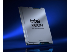
Intel also talked about the upcoming next generation Intel Xeon processor, which offers higher data throughput rates, considerably increased performance and highest levels of energy efficiency. The server chip has already won several tenders for High Performance Computing (HPC) environments: at the research centre in Juelich in Germany, the next generation Intel Xeon processors is set for a system with 1080 processing nodes and 8640 computing cores to enable realistic physical effects in running computer simulations in building and running the fusion experiment ITER which will support to have fusion as new source of energy in a long term perspective.
Intel server and workstation solutions will be powered by the "Nehalem EP" quad-core processors, which take advantage of the Hyperthreading technology (8 cores) QPI and support 3 channel DDR3 memory. In addition, Intel plans to release a six-core/12 threads CPU for servers called "Nehalem EX", mainly addressed for large-scale systems with 4 or 8 sockets.
Intels chairman, Dr. Craig Barrett, went into more detail about Intel Labs Europe (ILE), the recently announced organisation whose Munich location was formally opened on March 2nd 2009. Intel founded the ILE to drive the dialogue between Intel, the industry and academia and to catalyse and coordinate the company΄s European research and development activities.
Intel Labs Europe Intel is currently actively involved in 18 research facilities with around 800 scientists in Europe.


