TSMC Begins Construction on Gigafab In Central Taiwan
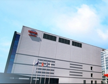
TSMC today held a ceremony in Taichungs Central Taiwan Science Park for Fab 15, TSMCs third 12-inch (300mm) Gigafab and an important milestone in the companys pledge to expand investment in Taiwan.
The ceremony was conducted by TSMC Chairman and CEO Dr. Morris Chang. "Science Parks have played a critical role in the development of Taiwans high-tech industry. They have also provided important support to TSMC as we grew to become a leading global semiconductor company with its roots in Taiwan," Dr. Chang said. "Over the past two decades, TSMC has flourished in the Hsinchu and Tainan science parks, and our groundbreaking for Fab 15 today sets the foundation for TSMC to reach new heights."
"TSMC has worked unceasingly to improve its technology leadership, manufacturing excellence, and customer partnership to join together with our fabless and IDM customers to forge a powerful competitive force in the semiconductor industry. This groundbreaking for Fab 15 in the Central Taiwan Science Park shows our commitment to providing our customers with advanced technology and satisfying their capacity needs. And as capacity in Fab 15 grows, it will create 8,000 high-quality job opportunities, demonstrating TSMCs dedication to corporate social responsibility," Dr. Chang added.
Fab 15 will be TSMCs third Gigafab, or fab with capacity of more than 100,000 12-inch wafers per month, and will also be TSMCs second Gigafab equipped for 28nm technology. Construction will be divided into four phases, and total investment over the next several years is expected to exceed NT$300 billion. TSMC is scheduled to begin equipment move-in for the Phase 1 facility in June 2011, with volume production of 40nm and 28nm technology products for customers in the first quarter of 2012. More advanced process nodes will be introduced as TSMCs technology development continues to advance.
TSMC will also continue to expand capacity at Fab 12 in Hsinchu and Fab 14 in Tainan. Combined capacity of Fab 12 and Fab 14 currently exceeds 200,000 12-inch wafers per month, and is scheduled to exceed 240,000 12-inch wafers per month by the end of this year.
Fab 15 will be TSMCs next "green fab" following Fab 12 and Fab 14, incorporating green concepts in energy conservation and pollution control in its design, including a process water conservation rate of 85%, reclamation of rainwater, recirculation and reuse of general exhaust heat, and development of solar power generation and LED lighting applications. TSMCs goal is to reach zero emissions of greenhouse gases.
Fab 15 Background Information
- Total area of site: 18.4 hectares
- Type of project: TSMCs third 12-inch Gigafab with two fab buildings and one office building.
- Building area: 430,000 square meters
- Clean room area: 104,000 square meters (approximately 14 soccer fields)

