NXP Releases Dual Supply Voltage ARM Cortex-M0 Microcontrollers For Mobiles, Tablets
NXP Semiconductors N.V. today announced its LPC1100LV series, an ARM Cortex-M0 microcontroller with dual supply voltage of 1.65V to 1.95V VDD and 1.65V to 3.6V VIO.
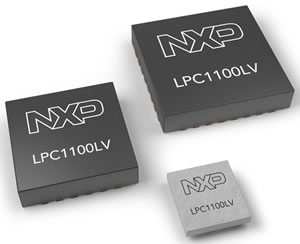
The LPC1100LV series offers 50 MIPS performance in a 2-mm x 2-mm footprint with over three times power reduction compared to similar 3.3V VDD devices. The LPC1100LV platform is specifically designed for battery-powered end applications ranging from mobile phones, tablets, Ultrabooks and mobile accessories to active cable, cameras, and portable medical electronics.
 Thanks to NXP's latest embedded Flash with 256-Byte erase sector and low leakage current, the LPC1100LV can handle linear current consumption at low clock frequency while reducing system power. For example, in a mobile system such as a smartphone, most system components are expected to remain mostly in sleep mode with very low current consumption. When a device is needed, fast wake-up and peak performance must be reached in a short amount of time. The LPC1100LV meets this demand with a 5-us wake-up time.
Performing More Demanding Tasks More Efficiently
NXP's LPC1100LV devices deliver 50 MIPS of performance compared to the 1 to 5 MIPS performance typical of 8/16-bit MCUs. This performance allows LPC1100LV to complete demanding tasks faster and to remain in active mode for a shorter period of time, further reducing the average current consumed by the device. Given the same task, LPC1100LV's 1.65V-1.95V VDD low-voltage input offers more than three times power reduction compared to other Cortex-M0 devices using 3.3V VDD input, and more than ten times compared to typical 8/16-bit MCUs. Sub-systems that can take special advantage of the LPC1100LV's MIPS performance include system security and authentication (including handling AES-256 encryption), system interface and controls (such as keypads and touchscreens), system peripheral controls (for audio and lighting), and for running software stacks (such as Bluetooth Low Energy radio). Small Footprint and Unique Level-Shifting Capability
The LPC1100LV is available in NXP?s tiny 2-mm x 2-mm Chip-Scale Package (WLCSP). Also available in a 5-mm x 5-mm HVQFN package and offering 1.8V VDD and 3.3V VIO dual voltage inputs for CPU and I/O, this option offers a level-shifting capability between SSP/SPI (3.3V) and I2C (1.8V). NXP is also offering customized combinations of SRAM, Flash and package for high-volume customers.
Other key specifications for the LPC1100LV devices include:
- Cortex-M0 CPU up to 50MHz
- 1.6-uA deep sleep current and 5-us wake-up time
- Up to 8 KB SRAM and 32 KB FLASH
- SPI, UART and I2C
- Up to 10-bit, 8-channel ADC with 400 ksps
- Two 32-bit Timers and two 16-bit Timers
- 12 MHz oscillator at 1% accuracy
- WL-CSP25, HVQFN24 and HVQFN33 package options (BGA available)
NXP is currently sampling the new microcontroler to its customers.


