Microsoft Provides Glimpse Of 24-core Processor For HoloLens
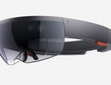
Microsoft today gave the first peek inside the custom vision processor it designed for its HoloLens augmented reality headset. The chip handles a trillion pixel-operations/second in a power budget lower than the 4W Intel Atom-based Cherry Trail SoC that acts as its host processor.
The HoloLens processing unit (HPU) fuses input from five cameras, a depth sensor and motion sensor, compacting and sending it to the Intel SoC. It also recognizes gestures and maps environments including multiple rooms.
Microsoft described the internal oarts of HoloLens earlier this year, but has not until now publicly detailed its HPU.
The TSMC 28nm chip packs 24 Tensilica DSP cores and 8 Mbytes cache into a 12x12mm package with 65 million transistors. A GByte of LPDDR3 is included in the HPU’s package.
The Tensilica cores were picked in part due to their flexibility. Microsoft added 300 custom instructions to the cores.
“If you can’t add custom instructions, the math density you wind up with is not what you need,” said Nick Baker, a distinguished technologist at Microsoft who described the HPU in a talk at the Hot Chips event in San Francisco.
The chip uses a mix of standalone accelerators and ones tightly coupled to its DSPs, getting an overall 200x speedup over a software-only version.
The chip is used in the $3,000 HoloLens developer’s kit released in March.


