Intel Unveils the Future Of Core, New GPUs, 3D Packaging With 'Foveros'
Intel demonstrated a new 3D packaging technology for face-to-face stacking of logic, scheduled to be available in the second half of next year. The company also tipped a new processor microarchitecture and a new graphics architecture.
The announcements were made at Intel “Architecture Day,” where top executives, architects and fellows revealed next-generation technologies and discussed progress on a strategy to power a data-intensive workloads for PCs and other smart consumer devices, high-speed networks, ubiquitous artificial intelligence (AI), specialized cloud data centers and autonomous vehicles.

Intel demonstrated a range of 10nm-based systems in development for PCs, data centers and networking, and previewed other technologies targeted at an expanded range of workloads.
The company also shared its technical strategy focused on six engineering segments: advanced manufacturing processes and packaging; new architectures to speed-up specialized tasks like AI and graphics; super-fast memory; interconnects; embedded security features; and common software to unify and simplify programming for developers across Intel’s compute roadmap.
3D packaging technology called “Foveros”
Intel has developed a way to stack its computing circuits on top of one another in a bid to regain the lead in chip manufacturing technology that it has lost to rivals like Taiwan Semiconductor Co Ltd in recent years. The company has fallen years behind schedule on its own plans.
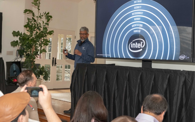
But Intel said it now has technology to stack computing circuits on top of each other and wire them together with speedy connections, enabling it to pack more onto a single chip. Stacking has been used in memory chips before, but Intel would be the first company to successfully stack the so-called "logic" chips that handle computing tasks, according to Raja Koduri, Intel's chief of chip architecture.
The 3D packaging technology, known as Foveros, will be available in the second half of next year, Intel said. It will also Intel break up its chip designs into smaller units called "chiplets" so that, for example, memory and computing chips can be stacked in different combinations.
Foveros is the next leap forward following Intel’s breakthrough Embedded Multi-die Interconnect Bridge (EMIB) 2D packaging technology, introduced in 2018.
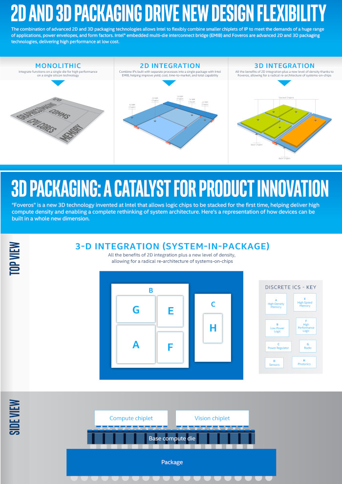
Unlike the passive interposer and stacked memory technologies currently available, Foveros extends the 3D packaging concept to include high-performance logic such as CPU, graphics and AI processors.
Koduri said Intel has already built products using the Foveros technology in response to customer requests. At the event, he showed what he called the first hybrid x86 architecture, featuring a 22FFL IO chip as the active interposer connected with TSVs to a 10nm die that contains both a single Sunny Cove core and four Atom cores in a 12x12x1mm Foveros package drawing just 2mW of standby power. This chip is obviously destined for mobile devices. It will support PCIe for M.2 as well as UFS.
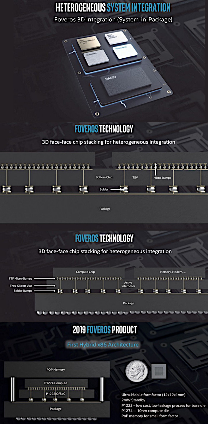
According to Koduri, Foveros technology will give designers greater flexibility to mix and match IP blocks with various memory and I/O elements in new form factors. It will allow products to be broken up into smaller chiplets, where I/O, SRAM and power delivery circuits can be fabricated in a base die and high-performance logic chiplets are stacked on top. He said the company plans to leverage the technology across the entire Intel product line.
Intel expects to launch a range of products using Foveros beginning in the second half of 2019. The first Foveros product will combine a high-performance 10nm compute-stacked chiplet with a low-power 22FFL base die. "It will enable the combination of world-class performance and power efficiency in a small form factor," according to Intel.
New Sunny Cove CPU Architecture
Intel also introduced Sunny Cove, Intel’s next-generation CPU microarchitecture designed to increase performance per clock and power efficiency for general purpose computing tasks, and includes new features to accelerate special purpose computing tasks like AI and cryptography. According to the company, Sunny Cove offers greater parallelism and features new algorithms to reduce latency and larger buffers and caches to optimize data-centric workloads. It will be the basis for Intel’s next-generation Xeon and Core later next year.
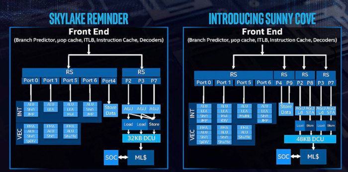
Sunny Cove features include:
- Enhanced microarchitecture to execute more operations in parallel.
- New algorithms to reduce latency.
- Increased size of key buffers and caches to optimize data-centric workloads.
- Architectural extensions for specific use cases and algorithms. For example, new performance-boosting instructions for cryptography, such as vector AES and
- SHA-NI, and other critical use cases like compression and decompression.
Intel says that Sunny Cove enables reduced latency and high throughput, as well as offers much greater parallelism that is expected to improve experiences from gaming to media to data-centric applications.
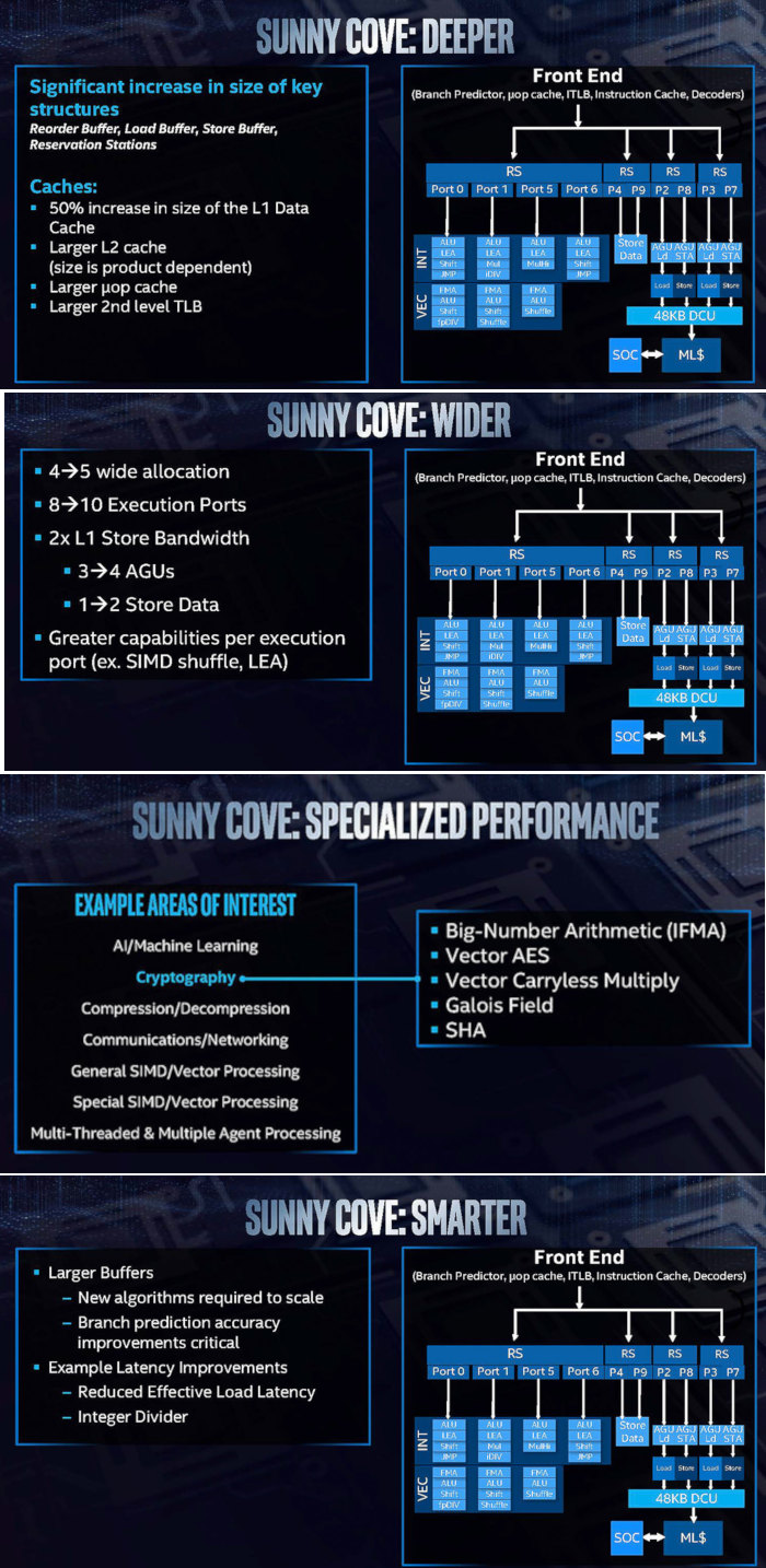
On the back end of the Sunny Cove microarchitecture design, Intel has increased cache sizes, making the execution of the core wider, increasing L1 store bandwidth, and other things.
The Sunny Cove core back end has a 48 KB L1 Data cache, upgraded from 32 KB. The L2 cache size has also been increased in both the Core and Xeon variants of Sunny Cove (256 KB and 1 MB respectively).
Intel also says that the micro-op (uOp) cache has increased from a 2048-entry design. The second level TLB size has also increased, which will help with machine address translation of recent addresses.
We can also see the execution ports to have increased from eight to ten, allowing more instructions to come out of the schedulers at one time. Port 4 and Port 9 is linked to a cycling data store, doubling that bandwidth, but also the AGU store capabilities have doubled, for which the increased L1-D size will help. There is also an allocation increase, moving from four to five. This means that the dispatch out of the reorder buffer can now hit five instructions per cycle, rather than four.
There are also changes in the execution ports between Skylake and Sunny Cove. Intel has equipped the Integer section of the core with more LEA units to help with memory addressing calculations. Port 1 gets the Mul unit from Skylake Port 5, probably for rebalancing purposes, but there is also an integer divider unit here. Also on the INT side is that Port 5’s multiply unit has become a ‘MulHi’ unit.
On the FP side, Intel has increased the shuffle resources.
Other updates to the core as listed from Intel include improvements to the branch predictor and a reduced ‘effective load latency’ (due to the TLB and L1-D).
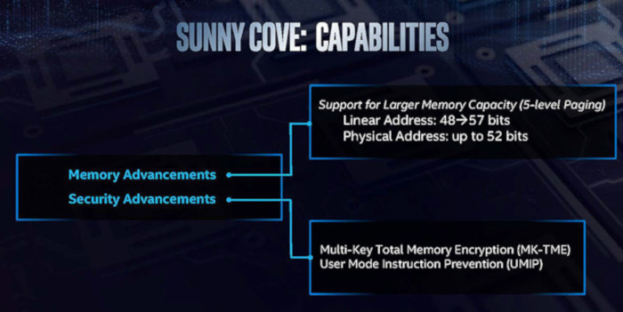
There are new instructions for the Sunny Cove core to help speed up specialist compute tasks. With the AVX-512 unit, the new core will support IFMA instructions for big arithmetic compute. Along the same lines, Vector-AES (supporting more AES concurrently) and Vector Carryless Multiply are also supported. SHA and SHA-NI instructrions are also added, along with Galois Field instructions.
For Sunny Cove, there is also built-in support for larger memory capacities. The paging table for main memory is now a five layer design, up from four layers, supporting a Linear Address space up to 57 bits and a physical address space up to 52 bits. According to Intel, this will allow the server processors to theoretically support 4 TB of memory per socket.
Gen11 integrated graphics
In graphics, Intel unveiled its new Gen11 integrated graphics — to be delivered in 10nm-based processors next year — and sketched out plans for a brand new architecture — X<e> — to serve as the foundation for both integrated and discrete graphics chips starting in 2020.
The new Gen11 integrated graphics come with 64 enhanced execution units, more than double previous Intel Gen9 graphics (24 EUs), designed to break the 1 TFLOPS barrier. This GT2 configuration has the 64 EUs split into four slices, with each slice being made of two sub-slices of 8 EUs a piece. Each sub-slice will have an instruction cache and a 3D sampler, while the bigger slice gets two media samplers, a PixelFE, and additional load/store hardware. Intel said that the FPU interfaces inside the EU are redesigned and it still has support for fast (2x) FP16 performance as seen in Gen9.5. Each EU will support seven threads, which means that the entire GT2 design will essentially have 512 concurrent pipelines. Intel has also redesigned the memory interface amd has increased the L3 cache of the GPU to 3 MB, a 4x increase over Gen9.5, and it is now a separate block in the unslice section of the GPU.
Other features include tile-based rendering, which Intel stated the graphics hardware will be able to enable/disable on a render pass basis. Meanwhile Intel's lossless memory compression has also improved, with Intel listing a best case performance boost of 10% or a geometric mean boost of 4%. The GTI interface now supports 64 bytes per clock read and write to increase throughput, which works with the better memory interface.
Coarse Pixel Shading is also supported. This allows the GPU to reduce the amount of total shading work required by shading some pixels on a less than 1:1 basis.
Intel says that the Gen11 design includes a ground up HEVC encoder design, with high quality encode and decode support. The company also stated that by using parallel decoders it can either support concurrent video streams or they can be combined to support a single large stream, and this scalable design will allow future hardware to push the peak resolutions up to 8K and beyond.
At the event, Intel showed Gen11 graphics nearly doubling the performance of a popular photo recognition application when compared to Intel’s Gen9 graphics. Gen11 will also feature Intel Adaptive Sync technology enabling smooth frame rates for gaming.
Intel also reaffirmed its plan to introduce a discrete graphics processor by 2020.
As we previoussly mentioned, Intel will use the Xe branding for its range of graphics. Xe will start from 2020 onwards, and cover the range from client graphics all the way to datacenter graphics solutions. Xe is exoected to go from entry to mid-range to enthusiast and up to AI, competing with the best the competition has to offer.
Intel stated that Xe will start on Intel’s 10nm technology and that it will fall under Intel’s single stack software philosophy, such that Intel wants software developers to be able to take advantage of CPU, GPU, FPGA, and AI, all with one set of APIs.
Sunny Cove cores and Gen11 graphics demos
Intel also ran a number of demos on a chip that was based on the new Sunny Cove cores and Gen11 graphics. The demos involved 7-Zip and gaming.
The 7-Zip demo showed how the new instructions such as Vector-AES and SHA-NI in Sunny Cove can give the processor a 75% boost in performance over an equivalent Skylake based platform at iso-frequency.
The other demo was Tekken 7, being run on a Sunny Cove + Gen11 machine and compared to a Skylake + Gen9 implementation. It looked smoother and went fully out of the 30 FPS minimums.

CPU Core Roadmaps
Intel also released both the Core architecture roadmap and the Atom architecture roadmap for the next few generations.
For the high performance Core architecture, Intel lists three new codenames over the next three years.

As we previously mentioned, the 10nm Sunny Cove will come to market in 2019.
It will be followed by Willow Cove core design in 2020, which will be most likely also built on 10nm. Intel lists the highlights here as a cache redesign (which might mean L1/L2 adjustments), new transistor optimizations (manufacturing based), and additional security features, likely referring to further enhancements from new classes of side-channel attacks.
Golden Cove rounds out the trio in 2021. Process is unknown, but we’re likely to see it on 10nm and or 7nm. Golden Cove brings an increase in single threaded performance, a focus on AI performance, and potential networking and AI additions to the core design. Security features also look like they get a boost.
The lower-powered Atom microarchitecture roadmap includes the Tremont microarchitecture for 2019, which focuses on single threaded performance increases, battery life increases, and network server performance.
Following Tremont will be Gracemont, which Intel lists as a 2021 product. Intel lists that Gracemont will have additional single threaded performance and a focus on increased frequency. This will be combined with additional vector performance, which likely means that Atom will get some wider vector units or support new vector instructions.
Beyond this will be a future ‘mont’ core in 2023.
“One API” Software

Intel announced the “One API” project to simplify the programming of diverse computing engines across CPU, GPU, FPGA, AI and other accelerators. The project includes a unified portfolio of developer tools for mapping software to the hardware that can best accelerate the code. A public project release is expected to be available in 2019.
Memory and Storage
Intel discussed updates on Intel Optane technology and the products based upon that technology. Intel Optane DC persistent memory is a new product that converges memory-like performance with the data persistence and large capacity of storage. The technology brings more data closer to the CPU for faster processing of bigger data sets like those used in AI and large databases. Its large capacity and data persistence reduces the need to make time-consuming trips to storage, which can improve workload performance. Intel Optane DC persistent memory delivers cache line (64B) reads to the CPU. On average, the average idle read latency with Optane persistent memory is expected to be about 350 nanoseconds when applications direct the read operation to Optane persistent memory, or when the requested data is not cached in DRAM.
For scale, an Optane DC SSD has an average idle read latency of about 10,000 nanoseconds (10 microseconds), a significant improvement. In cases where requested data is in DRAM, either cached by the CPU’s memory controller or directed by the application, memory sub-system responsiveness is expected to be identical to DRAM (<100 nanoseconds).
The company also showed how SSDs based on Intel’s 1 Terabit QLC NAND die move more bulk data from HDDs to SSDs, allowing faster access to that data.
Deep Learning Reference Stack
Intel is releasing the Deep Learning Reference Stack, an integrated, highly-performant open source stack optimized for Intel Xeon Scalable platforms. This open source community release is part of Intel's effort to ensure AI developers have easy access to all of the features and functionality of the Intel platforms. The Deep Learning Reference Stack is tuned and built for cloud native environments. With this release, Intel is enabling developers to quickly prototype by reducing the complexity associated with integrating multiple software components, while still giving users the flexibility to customize their solutions.
- Operating System: Clear Linux OS is customizable to individual development needs, tuned for Intel platforms and specific use cases like deep learning;
- Orchestration: Kubernetes manages and orchestrates containerized applications for multi-node clusters with Intel platform awareness;
- Containers: Docker containers and Kata containers utilize Intel Virtualization Technology to help secure container;
- Libraries: Intel Math Kernel Library for Deep Neural Networks (MKL DNN) is Intel’s highly optimized math library for mathematical function performance;
- Runtimes: Python providing application and service execution runtime support is highly tuned and optimized for Intel architecture;
- Frameworks: TensorFlow is a leading deep learning and machine learning framework;
- Deployment: KubeFlow is an open-source industry-driven deployment tool that provides a fast experience on Intel architecture, ease of installation and simple use.


