Future EUV to Move in Higher NA
During last week's International Electron Devices Meeting (IEDM,), ASML outlined the current statis of EUV lithography as well as the areas for improvement required in order EUV to remain sustain a healthy ecosystem as we move to smaller chip manufacturing nodes.
ASML's CEO, Martin van den Brink gave a plenary keynote titled "Continued Scaling in Semiconductor Manufacturing Enabled by Advances in Lithography." ASML is the only company that supplies EUV steppers.
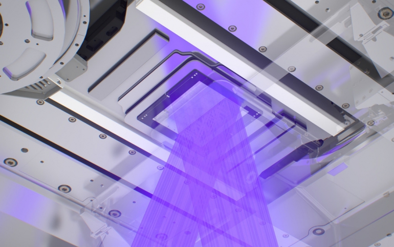
As a reminder, EUV is extreme-ultraviolet, a 13.5nm light source with reflective optics running in a vacuum produced by ASML. NA stands for numerical aperture, and is a measure of how much light gets captured and used by the optical system in the stepper. Bigger numbers are better.
A pellicle is a thin film that covers the reticle and ensures that any particle of contamination is kept out of the focal plane of the optics and so will not print. The issue here is the fast that EUV is absorbed by almost everything, so there are very few available materials. There is also another issue with reflective optics, the light path goes through the pellicle twice. So if the pellicle is 90% transmissive to the 13.5nm light, then only 81% (90% x 2) gets through.
All the mirrors in the optical path only reflect about 70% of the light. That is one reason for all the emphasis on source power and photoresist sensitivity: less than one percent of the light from the source makes it to the wafer.
Martin said that progress is required in several areas to enable single patterning to continue further. The goal is to maintain EUV single patterning all the way down to a minimum pitch below 20nm. This result would enable dimensional scaling to continue through the next decade at least.
He highlighted the areas that need further improvement.
First of all, he talked about the need for improved EUV photoresist materials with better resolution and simpler chemistry in order to reduce photon shot noise and chemical fluctuations. Have in mind that at these low dimensions, the placement of individual molecules of chemical amplification material starts to be important.
He also said that there is a need for an improved material for the EUV absorber on the mask (which is a mirror). TaBN is the current standard absorber, but for low-k1 imaging, the three-dimensional effect of the mask results in degradation of image contrast and edge placement errors.
The source power should be also be improved. ASML has demonstrated 500W in the lab, about twice the current number. The current ASML product, the NXE-3400C, is rated at 170 wafers per hour. So that is the status of the first generation of EUV lithography. 250W has been regarded as the minimum for EUV to have a high enough wafer throughput to be acceptable in high-volume manufacturing.
Last but not least, EUV should move the numerical aperture (NA) from the current 0.33 to 0.55.
One important issue that remains in place is the cost per layer. While the the economics for various levels of multi-patterning has been relatively low, the costs of the current EUV system (NXE EUV 0.33 NA) with single patterning and multi-patterning) is significantly higher. The goal is to be able to move to the next-generation high-NA system (EUV 0.55NA) using
just single patterning.
Martin said that by the end of Q2 there were 38 installed EUV systems.

