Advanced Foundry Technology Pushes Boundaries for the Industrial Revolution 4.0, Samsung Says
Samsung Electronics expects that foundries will play an increasingly important role as total solution providers, pushing the limits for broader engagement in the 4th industrial revolution era.
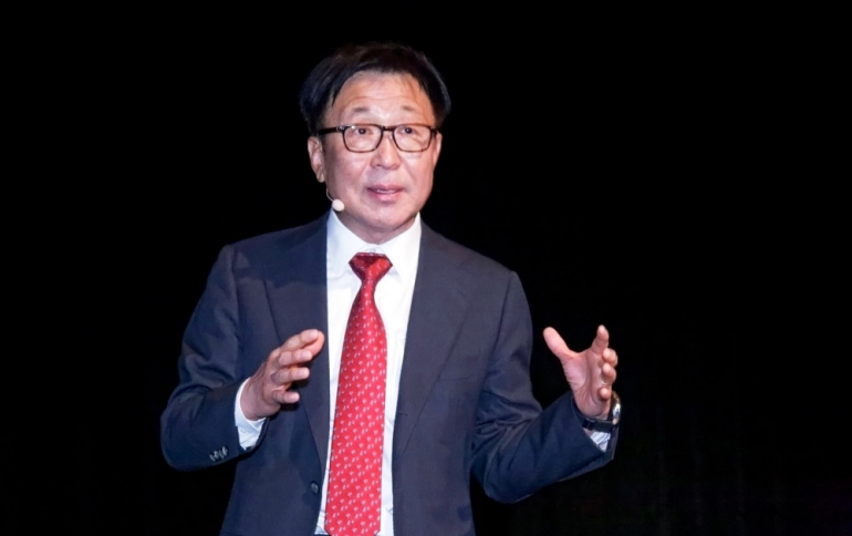
During a keynote speech at the 2018 IEEE International Electron Devices Meeting (IEDM), Dr. ES Jung, president and head of Foundry Business at Samsung Electronics, shared his vision that the next industrial revolution can only happen by the continuous evolution of semiconductor technology.
In his presentation “Fourth Industrial Revolution and Foundry: Challenges and Opportunities”, Dr. Jung explained that the evolution of advanced foundry technologies will be crucial to enable the design and manufacture of innovative semiconductor products that will take our everyday life into new and previously unthought-of directions.
New applications such as AI, cloud computing, autonomous vehicles, and smart home require high-level technologies including sophisticated design and system level optimization.
Dr. Jung discussed the increased complexities of semiconductor technology that has altered the role of the semiconductor foundry from a conventional wafer manufacturing business to a total solution provider. Today, foundries are providing value-added services, especially in the areas of design service and infrastructure, product engineering, and packaging/testing.
Semiconductors have evolved to be faster in speed, higher in density, and lower in power consumption, allowing a wide range of new applications. In addition, to analyze exponentially growing, unprecedented amounts of data, new memory architectures and completely new schemes of computation, such as neuromorphic computing, have to be developed.
“None of these technological advancements would have been possible without collaboration across the entire semiconductor industry” emphasized Dr. Jung. “This collaboration is paramount between material, equipment, electronic devices, government, universities, research centers, and consortiums, to ensure the success in the upcoming 4th industrial revolution.”
New Technological MilestonesDr. Jung also introduced some of recent research and development in future silicon technology, including MRAM, a non-volatile memory solution embedded in conventional logic process, and 3nm Gate-All-Around (GAA) technology.
MRAM is one of the examples of new semiconductor devices that consume much less power. As memory density becomes higher, MRAM’s power efficiency becomes more prominent, consuming only 0.5% of power compared to SRAM at 1,024Mb. MRAM also has smaller cell area, which allows design flexibility.
Samsung’s unique GAA technology called Multi-Bridge-Channel FET (MBCFET) uses vertically stacked multiple nanosheet channels. With variable width of nanosheet, this technology provides not only optimal performance and power characteristics, but also high design flexibility. Furthermore, MBCFET is fabricated using 90% or more of FinFET process with only a few revised masks, allowing easy migration.
Also with one of its newly published papers at 2018 IEDM, Samsung Electronics shared the development progress of 3nm, a successful demonstration of fully functioning high-density SRAM circuit. The development of Samsung’s first process node applying MBCFET technology is on schedule.


